

Semiconductor device and method for fabricating the same
- Summary
- Abstract
- Description
- Claims
- Application Information
AI Technical Summary
Benefits of technology
Problems solved by technology
Method used
Image

Examples
embodiment 1
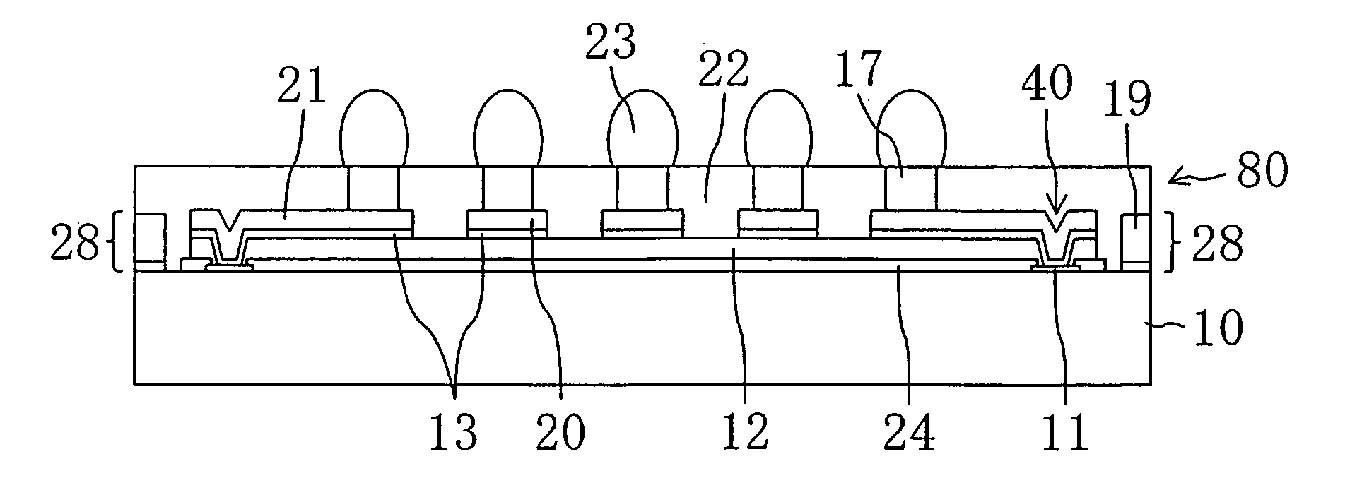
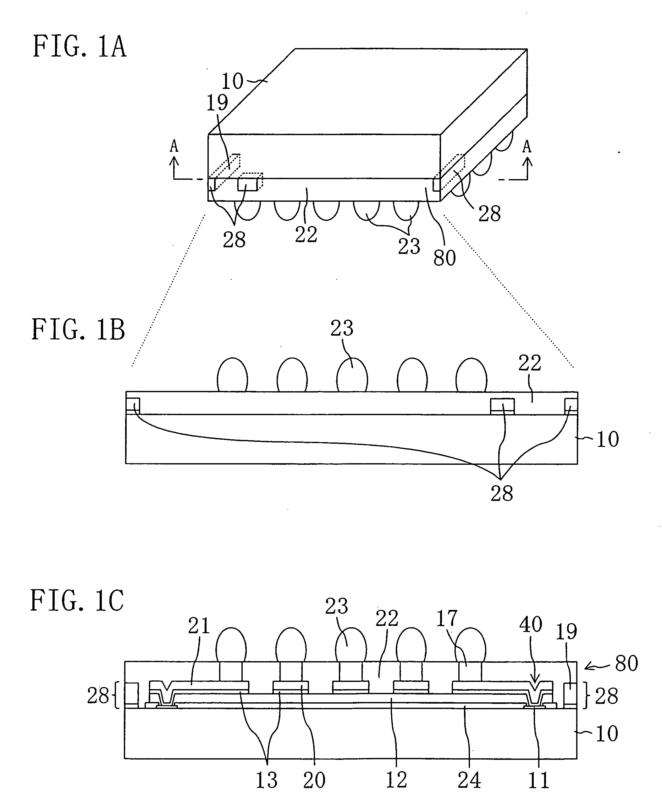
[0037]FIG. 1A is a perspective view showing a semiconductor device according to a first embodiment. FIG. 1B is a diagram showing the front side of FIG. 1A upside down. FIG. 1C is a cross-sectional view taken along the line A-A shown in FIG. 1A. In cross-sectional views described here and later, hatching is not given for the sake of the viewability of the drawings.
[0038] A semiconductor device of the present invention represents a CSP and is provided with a second insulating layer 22 on the surface of a semiconductor substrate 10 formed with a semiconductor integrated circuit composed of semiconductor elements such as transistors. The semiconductor device further comprises a plurality of external connection terminals 23, 23, . . . projecting from the surface of the second insulating layer 22. A plurality of mark parts 28, 28, 28 made of metal are exposed at parts of the second insulating layer 22 located on the side surfaces 80 of the semiconductor device. These mark parts 28, 28, 2...
embodiment 2
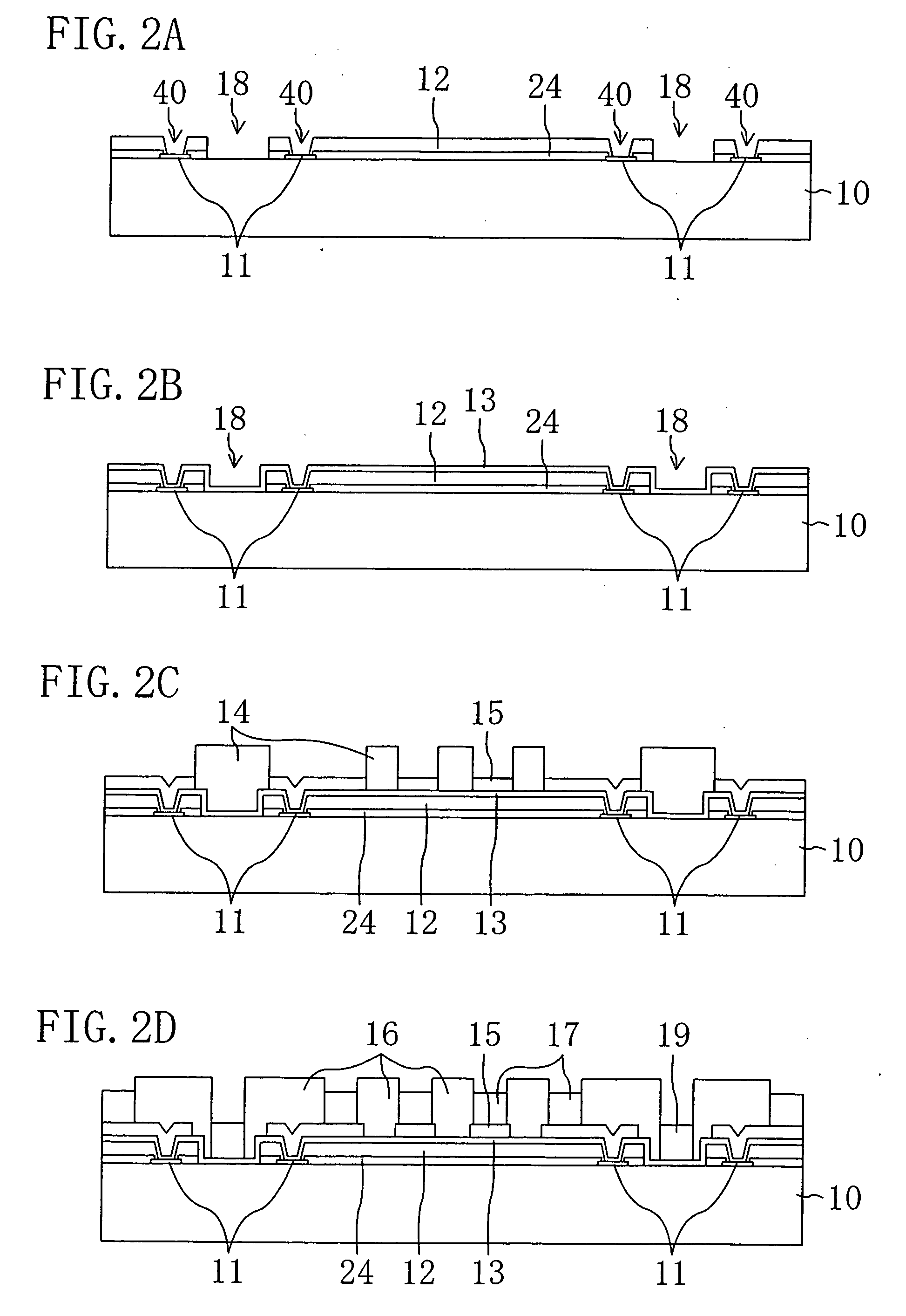
[0054]FIG. 4A is a cross-sectional view showing a semiconductor device according to a second embodiment. In this embodiment, first marks 19a are formed simultaneously with the formation of a layer of the first metal interconnects 21. Therefore, the first mark 19a is thinner than the first mark 19 of the first embodiment. The other structures, fabrication process steps, and effects and benefits are the same as in the first embodiment.
embodiment 3
[0055]FIG. 4B is a cross-sectional view showing a semiconductor device according to a third embodiment. In this embodiment, a second mark 19b is formed on each first mark 19a of the second embodiment simultaneously with the formation of the second metal interconnect 17. This can complicate the shape of each mark part 28 exposed at the associated side surface 80 of the semiconductor device 26, and allows a lot of information to be incorporated into the mark part 28 even when a small number of marks are provided. The other structures, fabrication process steps, and effects and benefits are the same as in the first embodiment.
[0056]FIG. 4C is a side view showing a semiconductor device in which both the first marks 19a and second marks 19b as described in the second and third embodiments are formed. As in this case, the different types of marks 19, 19a and 19b of the first through third embodiments may be formed as mixed in a single semiconductor device.
PUM
 Abstract
Description
Claims
Application Information