Superlattice nano-device and method for making same

a superlattice nano-device and nano-technology, applied in the field of nano-devices, can solve the problems of incompatibility of the vls method and the existing methods for synthesizing superlattice structures, and the difficulty of implementing the vls method,

Active Publication Date: 2007-03-15
TSINGHUA UNIV +1
View PDF11 Cites 29 Cited by
  • Summary
  • Abstract
  • Description
  • Claims
  • Application Information

AI Technical Summary

Benefits of technology

[0012] An embodiment of the present superlattice-based nanodevice includes a substrate, a one-dimensional nanostructure, a functional layer having a desired function, a conductive thin film electrode, and an insulating layer. The one-dimensional nanostructure extends from the substrate. The functional layer surrounds at least a portion of the one-dimensional nanostructure. The conducting thin film electrode surrounds the functional layer. The insulating layer is located between the substrate and the conductive thin film electrode and is thereby configured for creating an insulation therebetween. Further, the nanodevice can incorporate one or more functional units, each unit including a one-dimensional nanostructure and a respective functional layer. The units may or may not share the same conductive thin film electrode and / or insulating layer.

Problems solved by technology

However, some valuable / useful materials do not alloy with gold or platinum.
Therefore, possible candidates for the semiconductor material are limited, in that those materials incompatible with the catalyst cannot be applied to the superlattice nanowires.
Second, the VLS method for synthesizing the series-type superlattice nanowires is not compatible with the existing methods for synthesizing superlattice structures.
This need for precise control makes the VLS method difficult to implement.
However, the techniques for these processes is premature and / or developmental.

Method used


Image

  • Superlattice nano-device and method for making same
  • Superlattice nano-device and method for making same
  • Superlattice nano-device and method for making same

Examples


Embodiment Construction

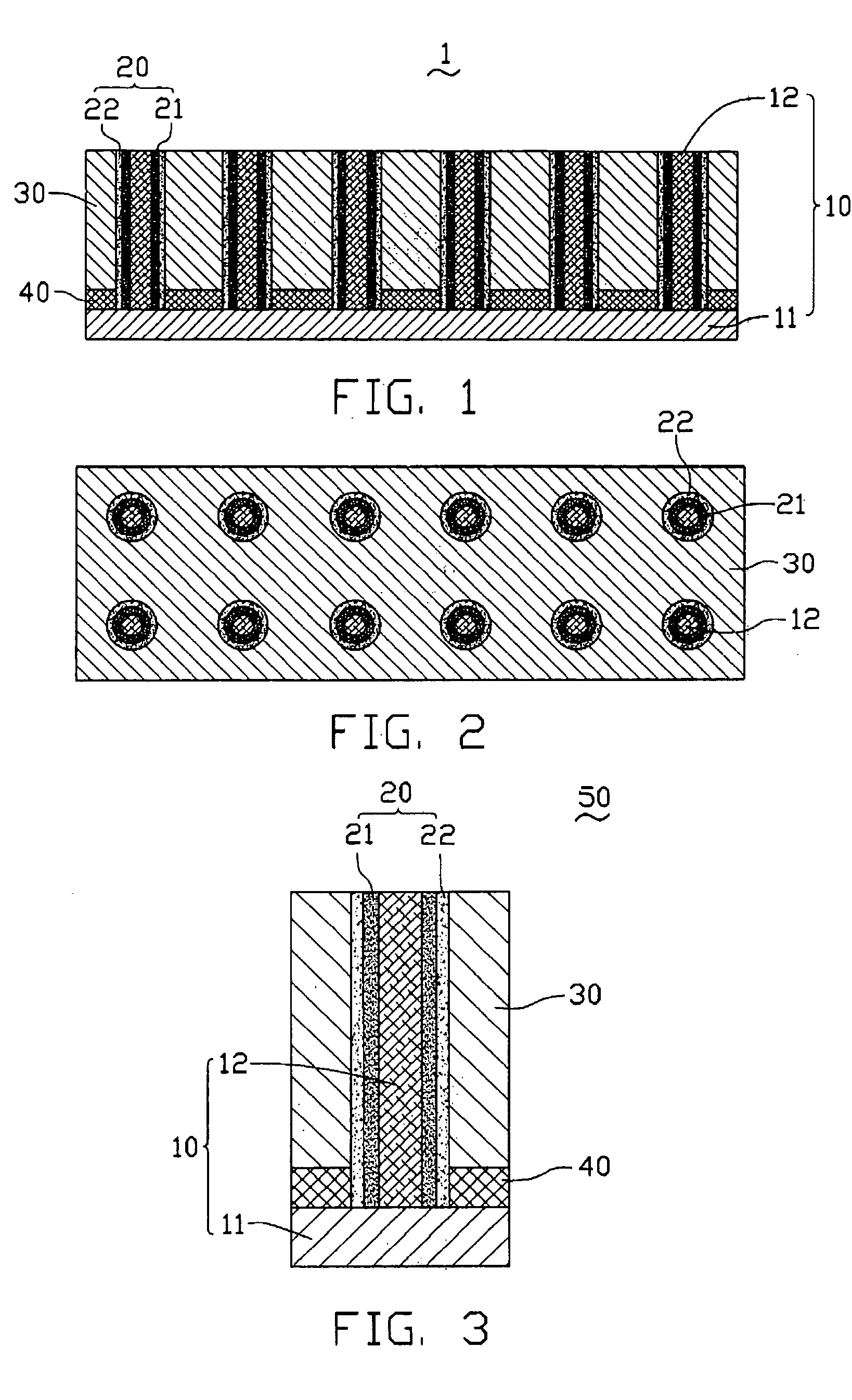
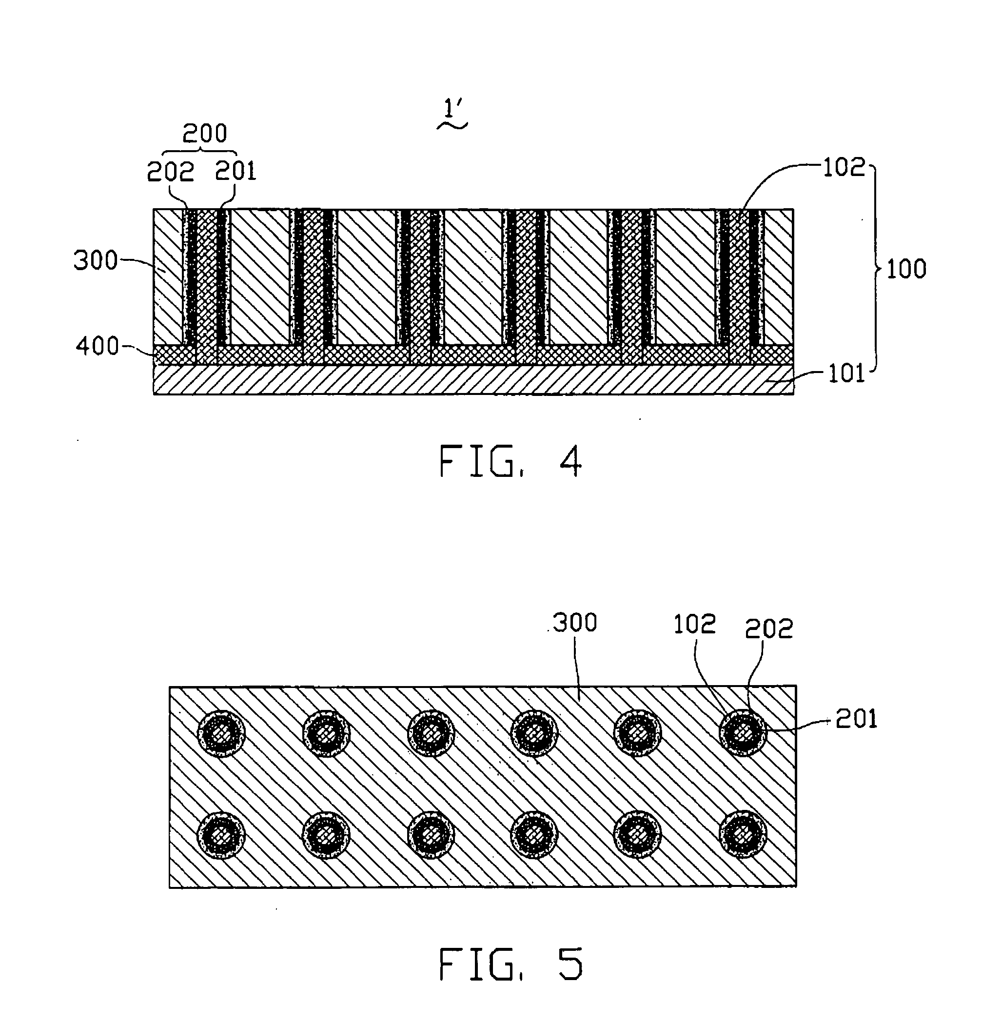
[0023] Reference will now be made to the drawings to describe preferred embodiments of the present superlattice-based nanodevice, in detail.

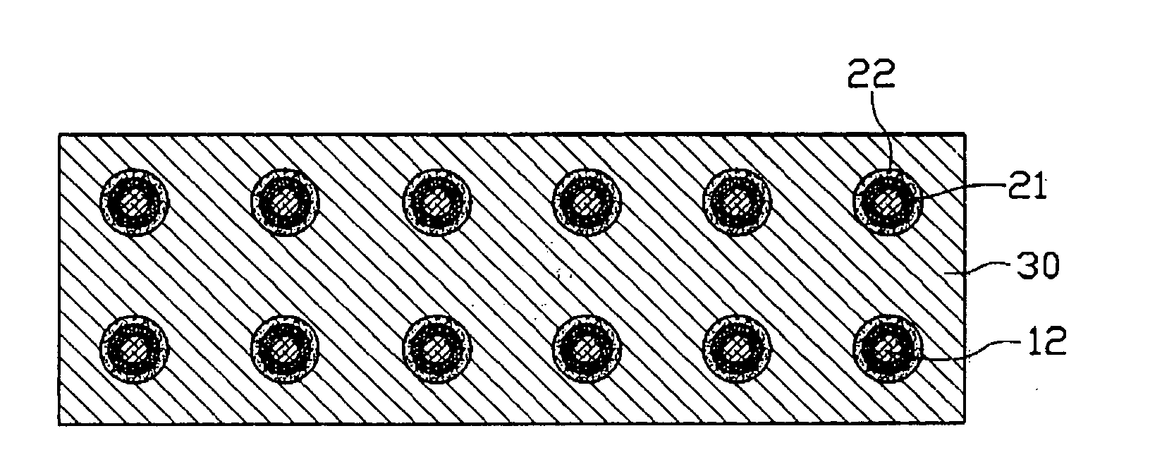
[0024] Referring to FIGS. 1 to 3, a nanodevice 1 according to a first embodiment is shown. The nanodevice 1 includes a number of units 50 (12 units are shown in FIGS. 1 and 2). The units 50 can be arranged, advantageously, in a regular pattern, such as an array or a matrix.

[0025] Each of the units 50 correspondingly includes a first electrode 10, a functional layer 20, a second electrode 30, and an insulating layer 40. The first electrode 10 includes a silicon substrate 11 and a one-dimensional nanomaterial, such as a silicon nanowire 12, formed on the silicon substrate 11. The functional layer 20 includes an annular first thin film 21 adjacently surrounding and contacting the silicon nanowire 12 and an annular second thin film 22 adjacently surrounding the first thin film 12. The functional layer 20 is, in turn, positioned on the silicon subs...


PUM

PropertyMeasurementUnit
aspect ratioaaaaaaaaaa
conductiveaaaaaaaaaa
electricallyaaaaaaaaaa

Abstract

A nanodevice (1) for a desired function includes a substrate (11), a one-dimensional nanostructure (12), a functional layer (20) having a desired function, a conductive thin film electrode (30), and an insulating layer (40). The one-dimensional nanostructure is operatively extends from the substrate. The functional layer is surrounds at least a portion of the one-dimensional nanostructure. The conducting thin film electrode is surrounds/encompasses the functional layer. The insulating layer is positioned between the substrate and the conductive thin film electrode, thereby electrically insulating the one from the other. Further, the nanodevice can incorporate one or more functional units 50, each unit including a one-dimensional nanostructure and a respective functional layer. The units may or may not share the same conductive thin film electrode and/or insulating layer.

Description

BACKGROUND OF THE INVENTION [0001] 1. Field of the Invention [0002] The present invention relates to nanodevices and methods for making them and, more particularly, to nanodevices having superlattice structures and methods for making such devices. [0003] 2. Related Art [0004] Nanotechnology is any technology which exploits phenomena and structures that occur at the nanometer scale, which is usually 0.1˜100 nanometers. Generally, nanomaterials involved in nanotechnology can be defined as those have nanostructured components at the nanometer scale. For example, nanomaterials with one dimension in the nanoscale are known as two-dimensional nanomaterials, such as a thin films or surface coatings having a thickness at nanometer scale; nanomaterials with two dimensions in the nanoscale are known as one-dimensional nanomaterials, such as nanowires and nanotubes; and nanomaterials with three dimensions in the nanoscale are known as zero-dimensional nanomaterials, such as particles or quantu...

Claims


Application Information

Patent Timeline
Patent Type & Authority Applications(United States)
IPC IPC(8): H01L33/00H01L21/00H01L33/06H01L33/08H01L33/32H01L33/38H01L33/40
CPCB82Y10/00H01L33/24H01L33/08H01L31/035236Y10S977/762
Inventor YAO, YUANCHU, WEI-GUOFAN, SHOU-SHAN
Owner TSINGHUA UNIV
Why Eureka
Try Eureka