LED module fabrication process with patterned transparent thin-film electrodes

A technology of LED modules and transparent films, which is applied in circuits, electrical components, semiconductor devices, etc., can solve problems such as LED light source failure, and achieve the effect of low production cost and transparent and beautiful products

Active Publication Date: 2011-12-21
SUZHOU SUNLIGHTS TECH
View PDF12 Cites 24 Cited by
  • Summary
  • Abstract
  • Description
  • Claims
  • Application Information

AI Technical Summary

Problems solved by technology

[0006] In the patent CN100514637, a method for connecting LED light sources and circuit electrodes is proposed. The wire-bonding process of traditional metal wires is used. Generally, gold wires, aluminum wires or copper wires are used. On a flexible substrate, this type of connection method is very convenient. It is easy to cause the LED light source to fail due to disconnection or deformation

Method used


Image

  • LED module fabrication process with patterned transparent thin-film electrodes
  • LED module fabrication process with patterned transparent thin-film electrodes
  • LED module fabrication process with patterned transparent thin-film electrodes

Examples


Embodiment 1

[0024] Transparent flexible substrate: The PET transparent flexible substrate with 180°C temperature resistance is ultrasonically cleaned with a 1:1 mixture of deionized water and alcohol, and baked in a drying oven at 100°C for 2 hours.

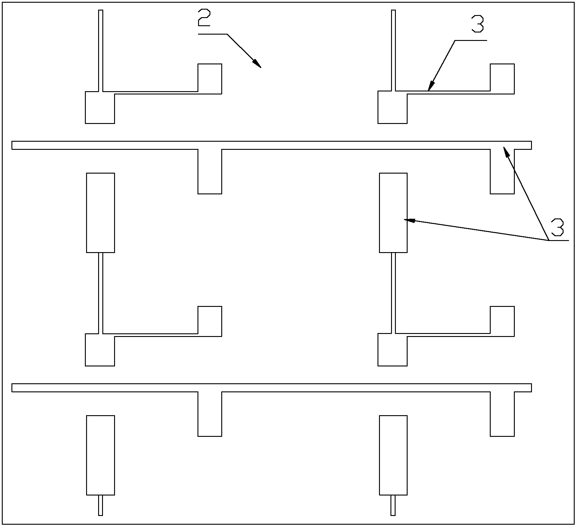
[0025] The first layer of insulating layer: Dissolve PVDF powder in dimethylacetamide solvent to prepare a dimethylacetamide solution containing PVDF with a concentration of 10%, and prepare a layer of PVDF on the above-mentioned transparent flexible substrate by a film-drawing process The transparent insulating polymer film is heated at 120°C and baked for 2 hours to form the first insulating layer 2; the surface of the first insulating layer 2 is made into a regular and uneven microstructure with a depth of 1 ~50nm, each time a layer of transparent insulating polymer film as an insulating layer is completed in the subsequent process, more than one nanoimprint process is performed.

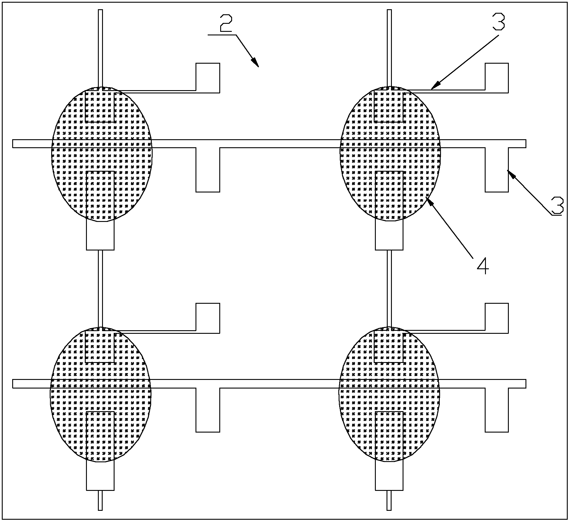
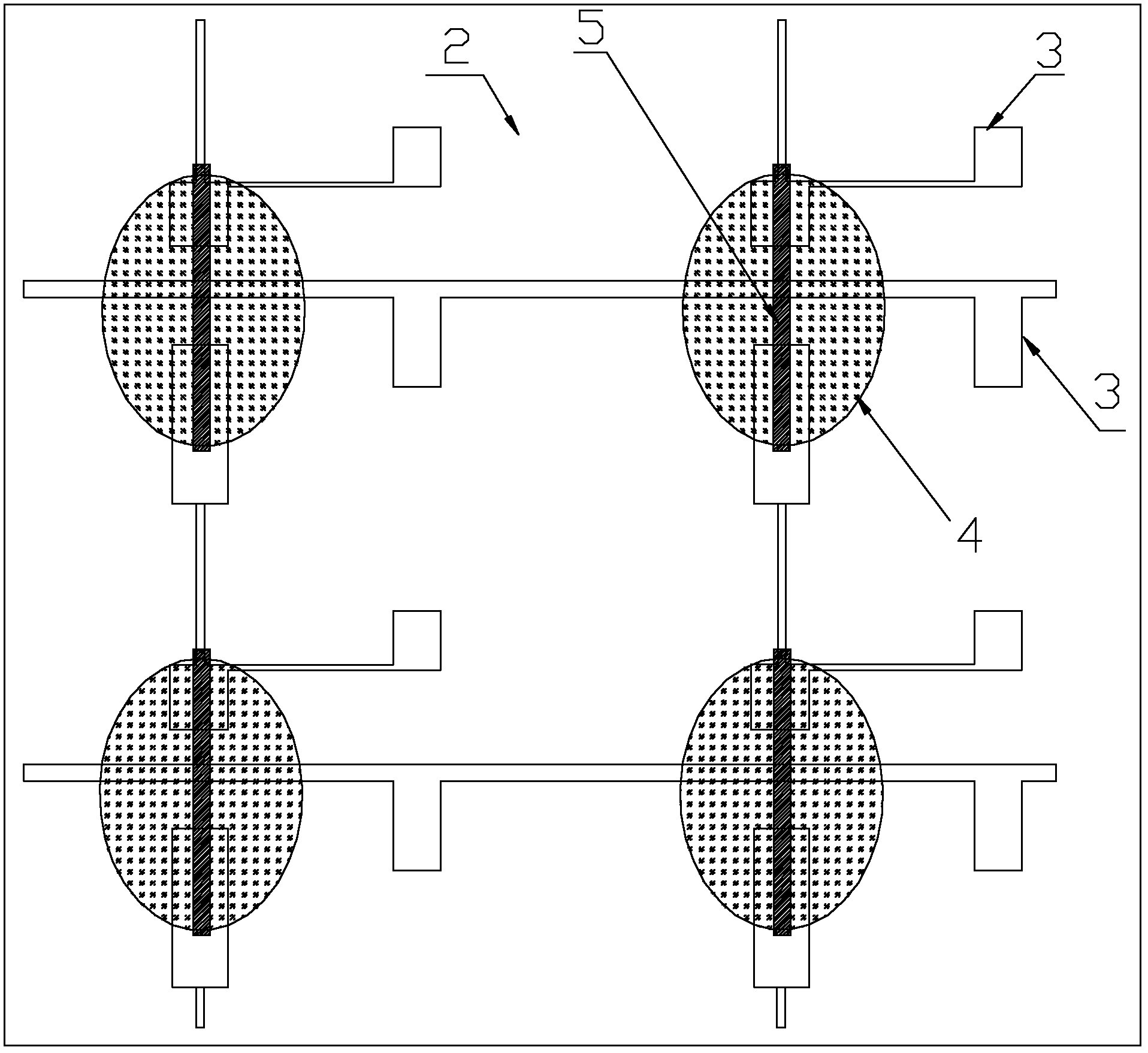
[0026]The first layer of patterned transparent conductive...

Embodiment 2

[0032] Transparent flexible substrate: The PVC film with 180°C temperature resistance is ultrasonically cleaned with a 1:1 mixture of deionized water and alcohol, and baked in a drying oven at 100°C for 2 hours, as a transparent flexible substrate for later use.

[0033] The first layer of insulating layer: prepare a PVA aqueous solution with a concentration of 8%, prepare a layer of PVA transparent insulating polymer film on the above-mentioned transparent flexible substrate through the glue-spinning process, and bake at 120°C for 2 hours to form the first layer of insulating layer 2.

[0034] The first patterned transparent conductive electrode: use the positive resist used in the traditional photolithography process to prepare a layer of film surface photoresist at the position where the conductive electrode is not needed by the screen printing process, and dry and bake at 80°C for 1 hour. Use the plasma surface treatment process to bombard the above-mentioned prepared film...


PUM

PropertyMeasurementUnit
lengthaaaaaaaaaa
diameteraaaaaaaaaa
lengthaaaaaaaaaa

Abstract

The invention relates to the technical field of a luminous display device, in particular to a novel graphical manufacturing technology of a nanometer material base transparent thin-film electrode; the manufacturing technology is characterized by comprising the following preparing steps of: a. preparing a raw material of a transparent conductive thin-film for standby application; using polyimide or one of PET (Polyethylene Terephthalate), PEN (Polyethylene Naphthalate), PC (Polycarbonate), PVC (Polyvinyl Chloride), PMMA (Polymethyl Methacrylate) and PES (Polyethersulfone) as a transparent flexibility substrate; b. preparing an insulating layer; c. preparing a graphical transparent conductive electrode; d. preparing a double-layer crossing or a multilayer graphical transparent conductive electrode; e. coating an LED (Light Emitting Diode); f. drying; and g. coating the film on the surface. Compared with the prior art, the manufacturing technology has the advantages that the novel thin-film electrode with the graphical function can be manufactured on the flexibly transparent base, the thin-film and the technology are combined with the manufacturing technology of a transparent LED (Light Emitting Diode) display device, a product is transparent and attractive and can be repeatedly bent and used and the manufacturing cost is low.

Description

technical field [0001] The invention relates to the technical field of light-emitting display devices, in particular to a patterned manufacturing process of a novel nanomaterial-based transparent film electrode. Background technique [0002] Light-emitting diode LED display is a device system that displays information by controlling the light emission of the LED matrix. Some special occasions, such as glass curtain walls, shop windows, three-dimensional billboards, stage backgrounds, hotels, airports and other environments require LED display modules to have good light transmission. Display installation, handling and maintenance. [0003] In the published patent CN100481448C, a transparent light-emitting diode display for presenting information in motor vehicles is provided, which uses glass coated with a transparent conductive oxide film as a conductive path as a flexible substrate for display devices; patent CN 201622784U designs A transparent display based on a glass pl...

Claims


Application Information

Patent Timeline
Patent Type & Authority Applications(China)
IPC IPC(8): H01L33/00
Inventor 张哲娟孙卓
Owner SUZHOU SUNLIGHTS TECH
Why Eureka
Try Eureka