Manufacturing technology of LED (Light Emitting Diode) module with graphical transparent thin-film electrode
A technology of LED modules and transparent films, applied in circuits, electrical components, semiconductor devices, etc., can solve problems such as failure of LED light sources, and achieve the effect of low production cost and transparent and beautiful products.
- Summary
- Abstract
- Description
- Claims
- Application Information
AI Technical Summary
Problems solved by technology
Method used
Image
Examples
Embodiment 1
[0024] Transparent flexible substrate: The PET transparent flexible substrate with temperature resistance of 180°C is ultrasonically cleaned with a 1:1 mixture of deionized water and alcohol, and baked in a drying oven at 100°C for 2 hours.
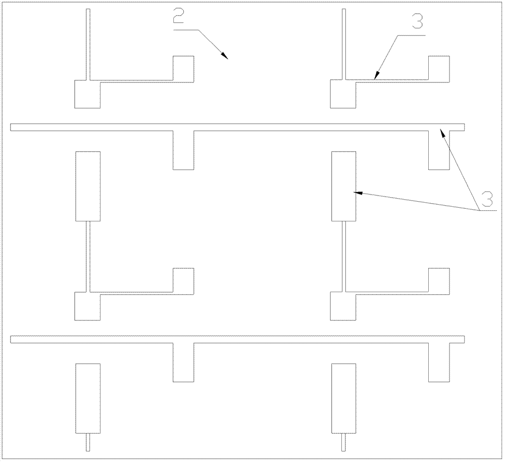
[0025] The first layer of insulating layer: Dissolve PVDF powder in dimethylacetamide solvent to prepare a dimethylacetamide solution containing PVDF with a concentration of 10%, and prepare a layer of PVDF on the above-mentioned transparent flexible substrate by a film-drawing process The transparent insulating polymer film is baked at 120°C for 2 hours to form the first insulating layer 2; the surface of the first insulating layer 2 is made into a regular and uneven microstructure by nanoimprinting process, and the microstructure depth is 1 ~50nm, each time a layer of transparent insulating polymer film as an insulating layer is completed in the subsequent process, more than one nanoimprint process is performed.
[0026]The first layer ...
Embodiment 2
[0032] Transparent flexible substrate: The PVC film with 180°C temperature resistance is ultrasonically cleaned with a 1:1 mixture of deionized water and alcohol, and baked in a drying oven at 100°C for 2 hours, as a transparent flexible substrate for later use.
[0033] The first layer of insulating layer: prepare a PVA aqueous solution with a concentration of 8%, prepare a layer of PVA transparent insulating polymer film on the above-mentioned transparent flexible substrate through the glue-spinning process, and bake at 120°C for 2 hours to form the first layer of insulating layer 2.
[0034] The first patterned transparent conductive electrode: use the positive resist used in the traditional photolithography process to prepare a layer of film surface photoresist at the position where the conductive electrode is not needed by the screen printing process, and dry and bake at 80°C for 1 hour. Use the plasma surface treatment process to bombard the above-mentioned prepared film...
PUM
| Property | Measurement | Unit |
|---|---|---|
| length | aaaaa | aaaaa |
| diameter | aaaaa | aaaaa |
| length | aaaaa | aaaaa |
Abstract
Description
Claims
Application Information


