Magnetic switching element and signal processing device using the same

a switching element and signal processing technology, applied in semiconductor devices, digital storage, instruments, etc., can solve the problems of power saving disadvantages, fatal energy loss of micro machines,

Inactive Publication Date: 2007-03-15
KK TOSHIBA
View PDF10 Cites 16 Cited by
  • Summary
  • Abstract
  • Description
  • Claims
  • Application Information

AI Technical Summary

Problems solved by technology

For this reason, energy loss is fatal for the micro machine.
However, as for the switching element such as the MOSFET or diode, an ON / OFF resistance ratio is small and ON resistance is large, and thus, it is disadvantageous for accomplishment of power saving.

Method used


Image

  • Magnetic switching element and signal processing device using the same
  • Magnetic switching element and signal processing device using the same
  • Magnetic switching element and signal processing device using the same

Examples


first embodiment

[0072] (1) First Embodiment

[0073] A first embodiment relates to a magnetic switching element in a state that a channel of an input signal IN and a channel of an output signal OUT are overlapped with each other, the input signal IN and output signal OUT cause the switch to operate ON / OFF.

[0074] A. Basic Structure

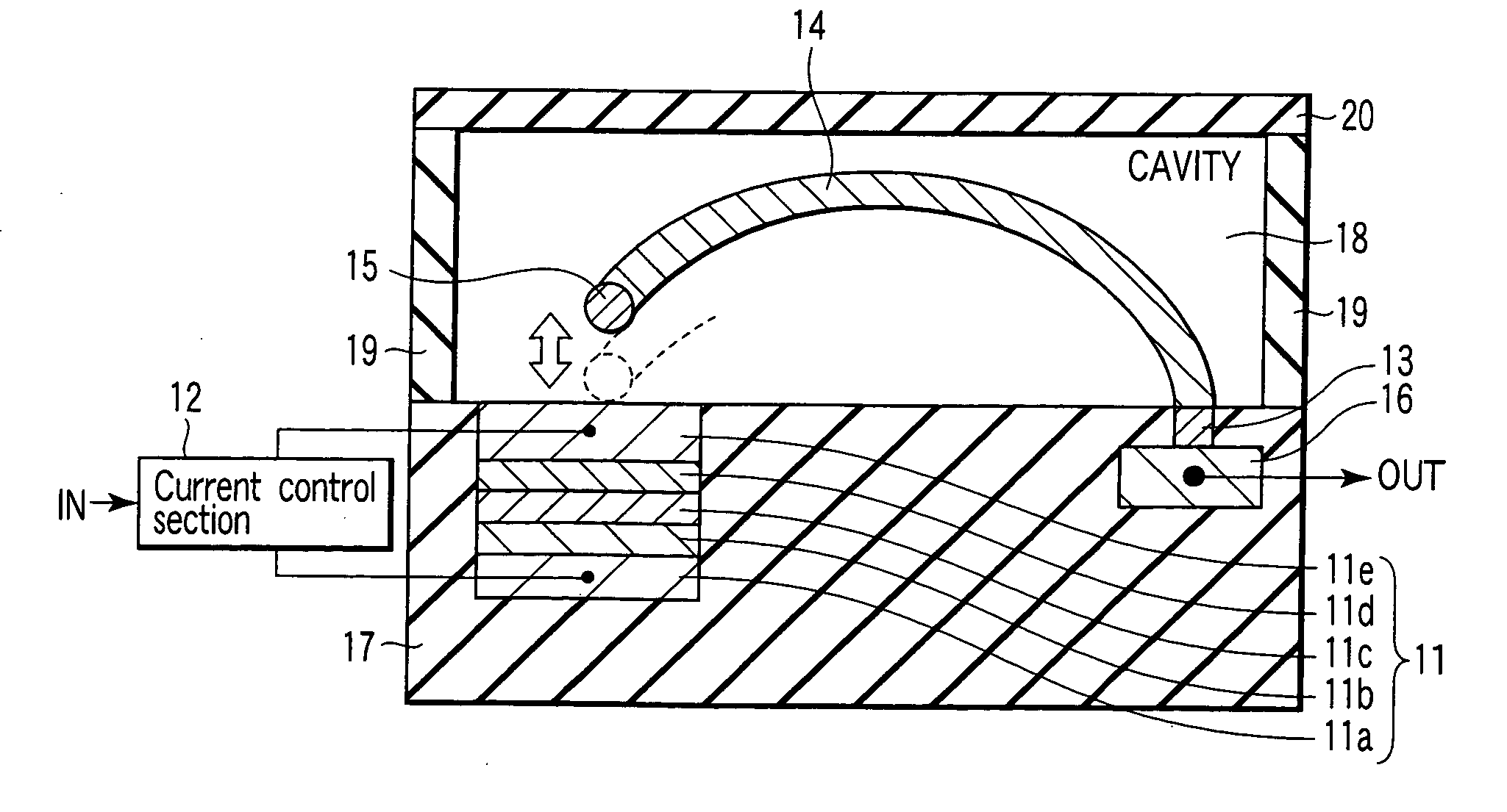
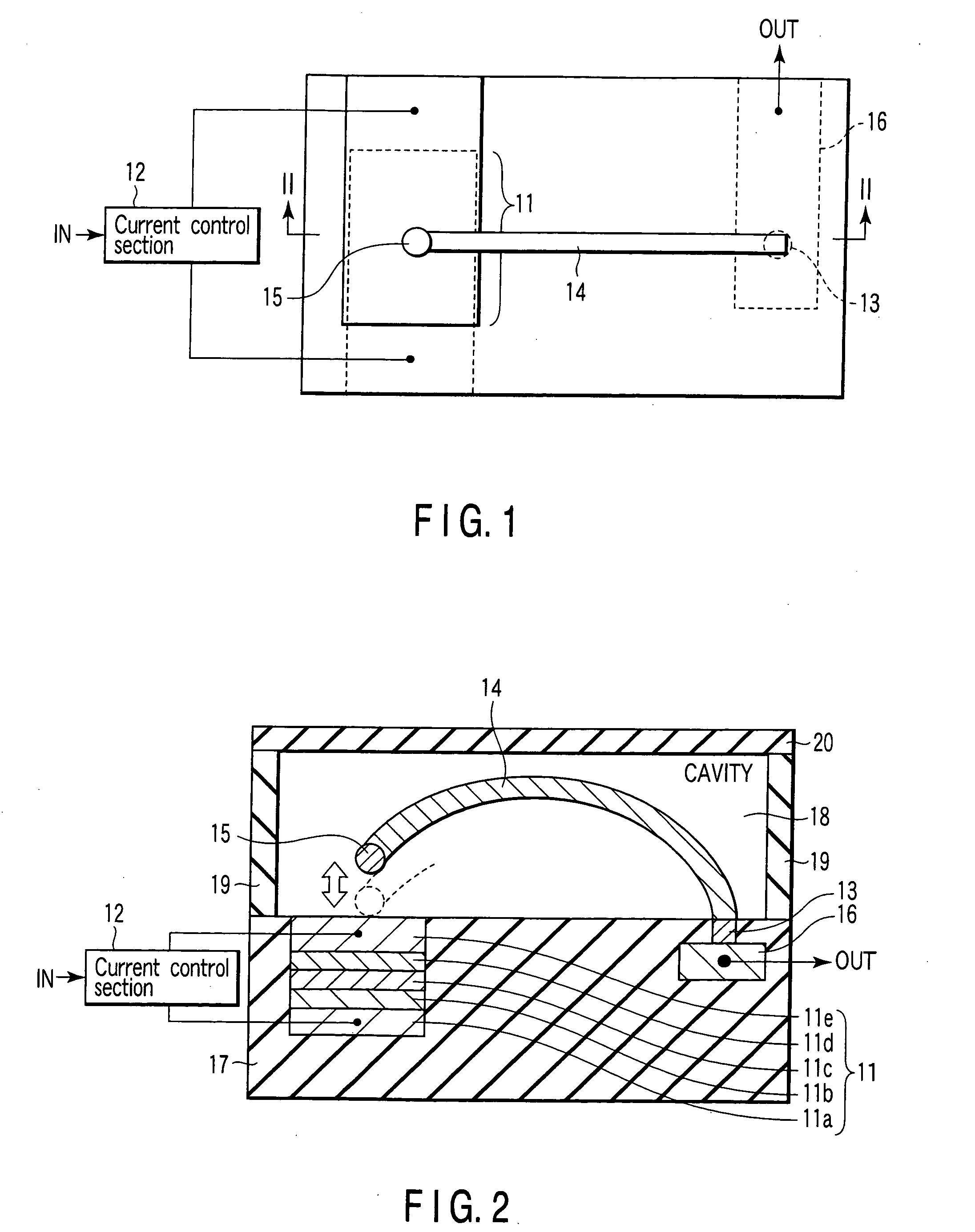
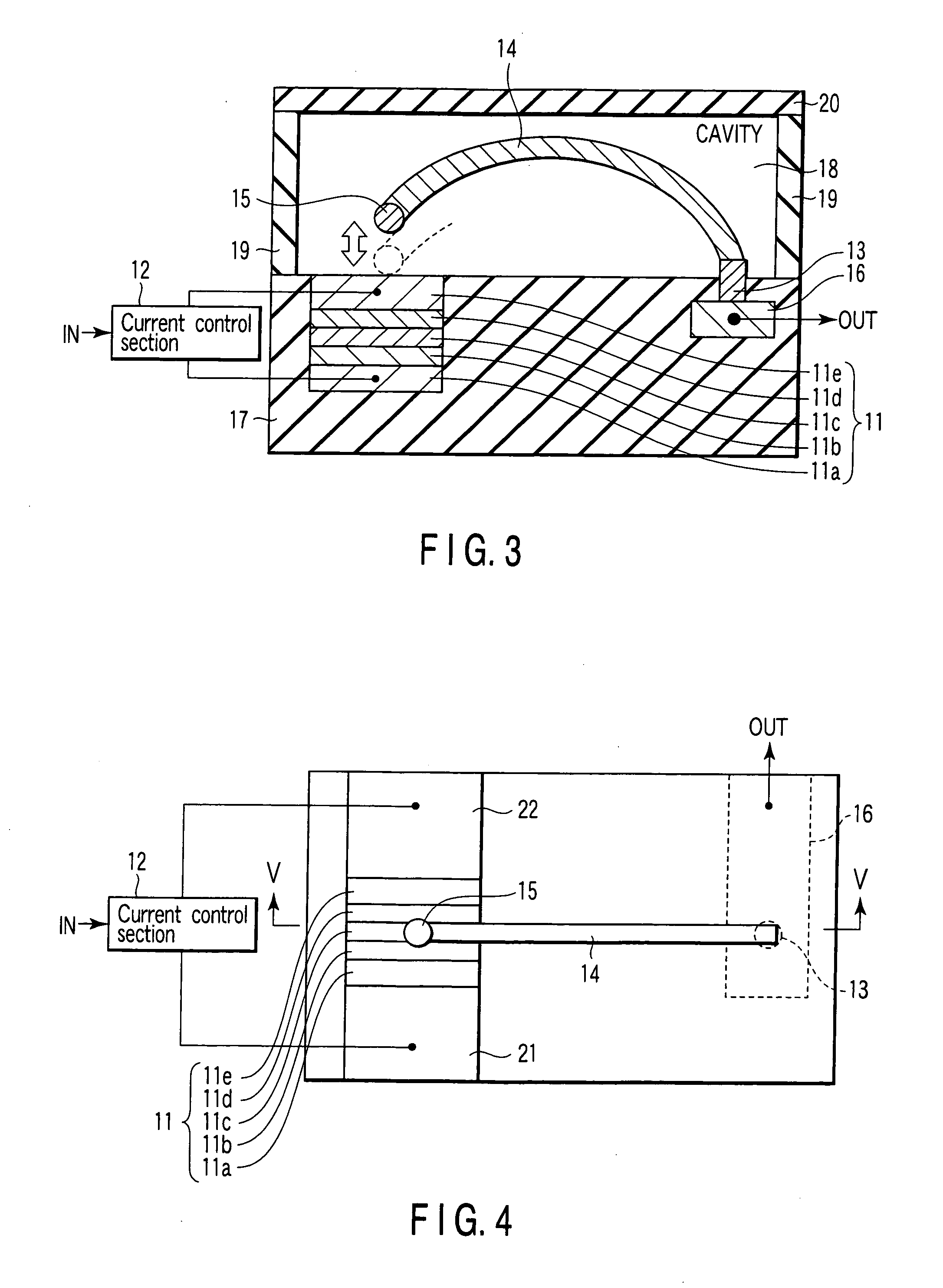
[0075]FIG. 1 is a plan view of the magnetic switching element according to the first embodiment. FIG. 2 is a cross sectional view taken along a line II-II of FIG. 1.

[0076] A magnetic field generation section 11 is composed of first and second electrodes 11a, 11b and a magnetic element arranged between the electrodes. The magnetic element is composed of magnetic layers 11b, 11d and a non-magnetic layer 11c arranged between the magnetic layers.

[0077] One of the two magnetic layers 11b, 11d functions as a magnetization fixed section whose magnetization direction is fixed, while the other thereof functions as a magnetization free section whose magnetization direction is chang...

second embodiment

[0114] (2) Second Embodiment

[0115] A second embodiment relates to a magnetic switching element in which a channel of an input signal IN and a channel of an output signal OUT are separated from each other, the signals causing a switch to perform ON / OFF operation.

[0116] A. Basic Structure

[0117]FIG. 6 is a plan view of the magnetic switching element according to the second embodiment. FIG. 7 is a cross sectional view taken along a line VII-VII of FIG. 6.

[0118] A structure of a magnetic field generation section 11 is the same as that of the first embodiment, and is composed of first and second electrodes 11a, 11e, and a magnetic element arranged between the electrodes. The magnetic element is composed of magnetic layers 11b, 11d, and a non-magnetic layer 11c arranged between the magnetic layers.

[0119] In the present embodiment, the channel of the input signal IN and the channel of the output signal OUT are separated from each other. For this reason, the second electrode 11e of the m...

third embodiment

[0156] (3) Third Embodiment

[0157] A third embodiment has a characteristic in the conductive tube. In the first and the second embodiments, the conductive tube is caused to grow from a flat surface substantially in parallel to a surface beneath which the magnetic field generation section is buried. However, in the third embodiment, the conductive tube is formed substantially in parallel to a surface beneath which a magnetic field generation section is buried.

[0158] A. Basic Structure

[0159]FIG. 11 is a plan view of a magnetic switching element according to the third embodiment. FIG. 12 is a cross sectional view taken along a line XII-XII of FIG. 11.

[0160] A structure of the magnetic field generation section 11 is the same as that of the first embodiment. That is, the respective layers constituting the magnetic field generation section 11 may be stacked in the vertical direction as shown in FIGS. 1 and 2, or alternatively, may be stacked in the lateral direction as shown in FIGS. 4 ...


PUM


Abstract

A magnetic switching element according to an example of the present invention includes a magnetic element, first and second electrodes which put the magnetic element therebetween, a current control section which is connected to the first and second electrodes, the current control section controlling a magnetization direction of a magnetization free section in such a manner that a current is made to flow between the magnetization free section and the magnetization fixed section, a movable conductive tube having a fixed end and a free end, and a third electrode connected to the fixed end of the conductive tube. A switching operation is performed in such a manner that a spatial position of the conductive tube is caused to change depending on the magnetization direction of the magnetization free section.

Description

CROSS-REFERENCE TO RELATED APPLICATIONS [0001] This application is based upon and claims the benefit of priority from prior Japanese Patent Application No. 2005-262579, filed Sep. 9, 2005, the entire contents of which are incorporated herein by reference. BACKGROUND OF THE INVENTION [0002] 1. Field of the Invention [0003] The present invention relates to a switching element which uses a magnetic force. [0004] 2. Description of the Related Art [0005] A switching element using a semiconductor represented by a MOSFET or a diode can be ultra-miniaturized and integrated, and therefore, such a switching element becomes one of indispensable devices in various existing electronic devices. [0006] Meanwhile, development advances concerning microscopic machine such as a micro-machine or a nano-machine due to an improvement of a nano-technology of late. For example, in a medical field, a nano-machine will be materialized in the not-too-distant future. [0007] By the way, a drive source of such a...

Claims


Application Information

Patent Timeline
Patent Type & Authority Applications(United States)
IPC IPC(8): H01L29/74
CPCB82Y10/00G11C11/16H01H1/0094G11C23/00G11C2213/71G11C13/025Y10S977/725Y10S977/943
Inventor NAKAMURA, SHIHOMOTOI, YUICHIHANEDA, SHIGERUMORISE, HIROFUMIHIRAI, TAKAHIRO
Owner KK TOSHIBA
Why Eureka
Try Eureka