Method and apparatus for detecting defects

a technology of defects and grayscale depth, applied in the field of microfine pattern inspection, can solve the problems of insufficient large grayscale depth of defects, and time-consuming to find optimal conditions, so as to reduce the grayscale depth of pseudo defects, improve the grayscale depth of defects, and quick select

Inactive Publication Date: 2007-03-15
HITACHI HIGH-TECH CORP
View PDF9 Cites 60 Cited by
  • Summary
  • Abstract
  • Description
  • Claims
  • Application Information

AI Technical Summary

Benefits of technology

[0014] With this invention, it is possible to quickly select an optical condition that improves the grayscale depth of defects and reduces the grayscale depth of pseudo defects, thereby realiz

Problems solved by technology

Further, on the wafer to be inspected there are various kinds of defects as well as pseudo defects that are preferably not detected.
Therefore, when detecting defects by using a particular wavelength, as disclosed in JP-A-2004-55695, some kind of defects may get a large grayscale depth and some kind may fail to get a sufficient grayscale depth.
When a plurality of optical means are used to further increase the grayscale depth of defects, there are problems that fin

Method used


Image

  • Method and apparatus for detecting defects
  • Method and apparatus for detecting defects
  • Method and apparatus for detecting defects

Examples


embodiment 1

[Embodiment 1]

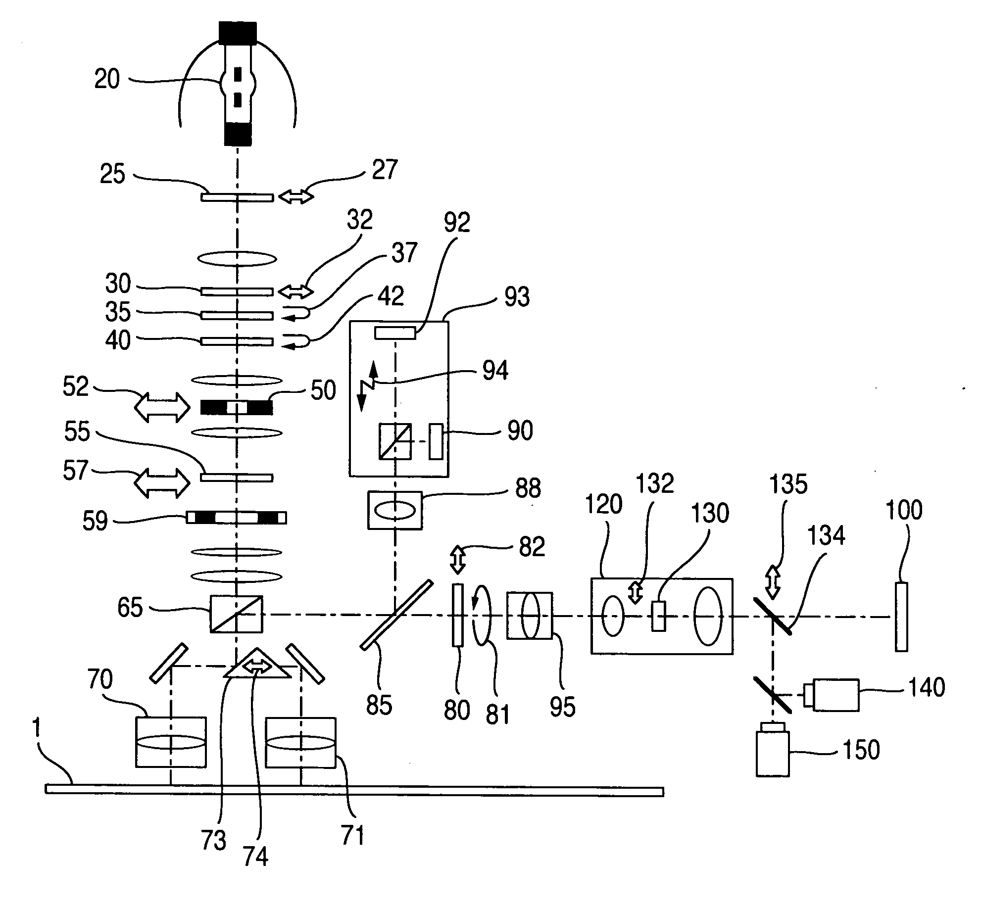
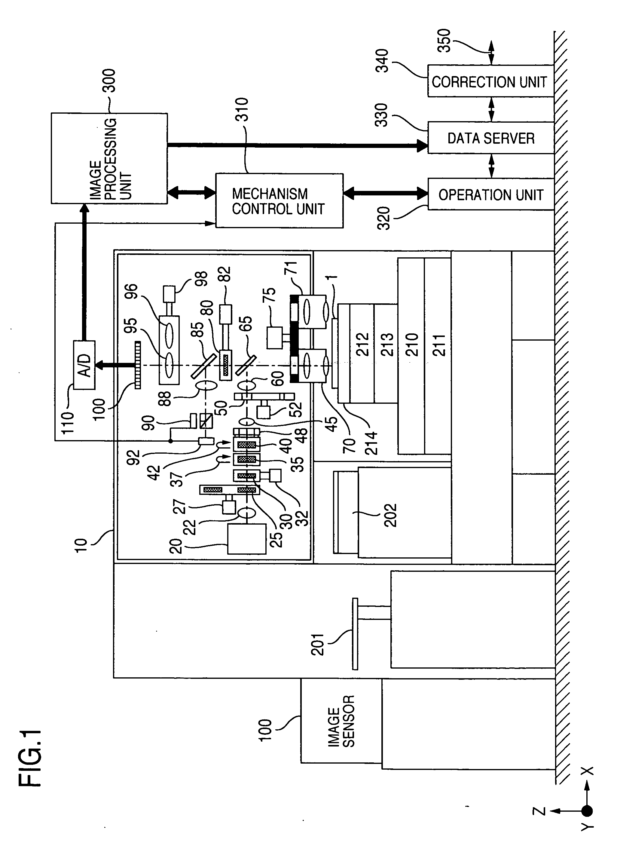
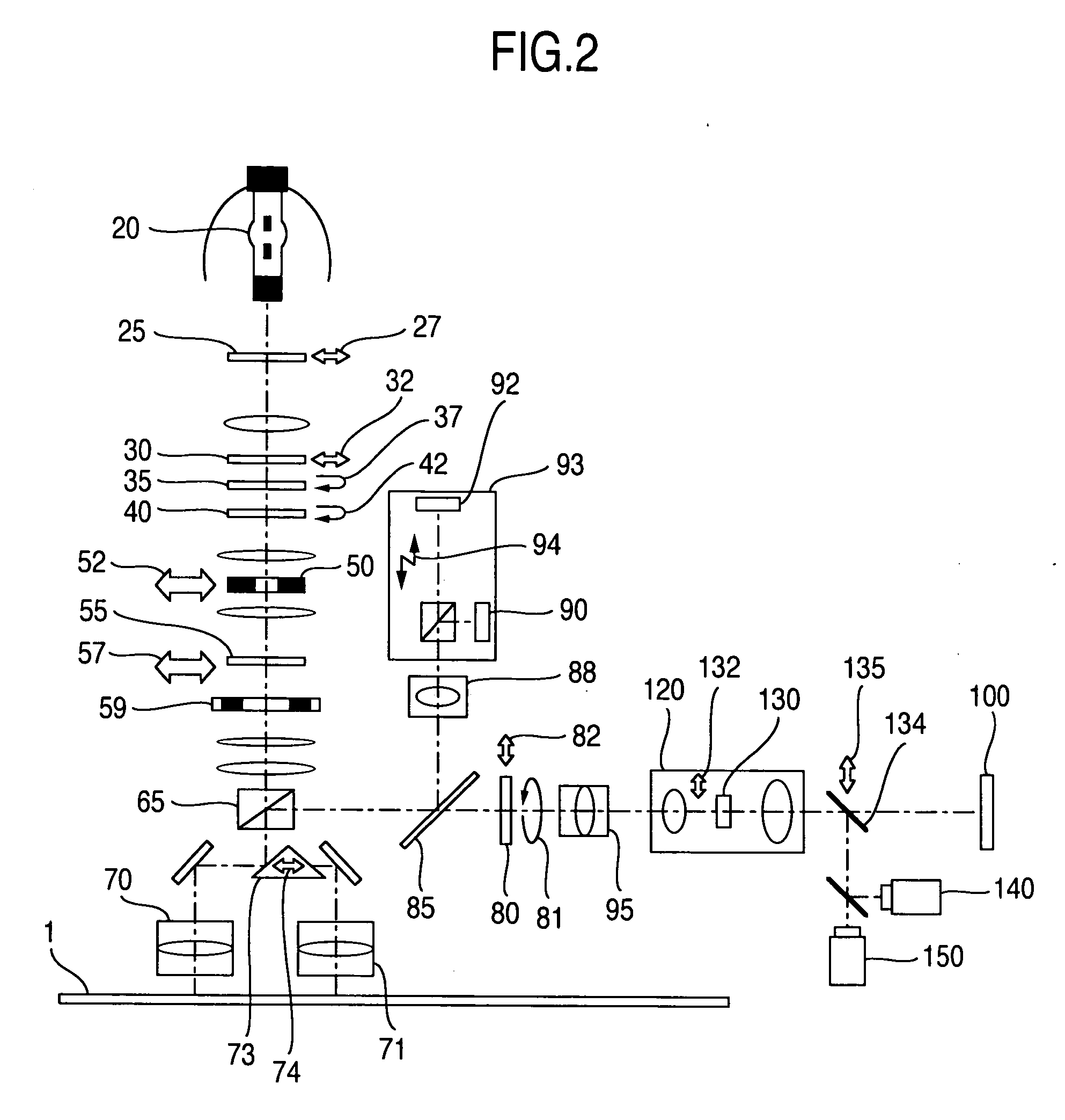
[0031] A basic construction of an optical defect inspection apparatus according to this invention is shown in FIG. 1. A wafer 1 is stored in a hoop 100 and loaded into a notch detection unit 202 by a wafer loader 201. The wafer 1, that has its notch detected by the notch detection unit 202 and is prealigned, is attracted to a wafer chuck 214 mounted on an X stage 210, a Y stage 211, a Z stage 212 and a θ stage 213. Above the wafer 1 is arranged an optical system 10 to detect an image of a wafer surface (this figure shows a construction of a bright field detection optical system using a falling light illumination). A light source 20 emits light of a wide wavelength band and may use such lamps as Xe lamp, ultrahigh pressure Hg lamp, Hg—Xe lamp and halogen lamp. Light from the lamp 20 passes through a lens 22, a wavelength selection filter 25 and a polarizer 30. The wavelength selection filter 25 is, for example, an interference filter or a colored glass having an absorbi...

embodiment 2

[Embodiment 2]

[0100] A detection system of microscope is largely classified into a bright-field detection and a dark-field detection. Depending on the detection principle, some defects are easily detected and some are not. For example, the bright-field detection system can easily detect small-step thin film residues, fine shorted defects and pattern shape anomalies. The dark-field detection system can advantageously detect stepped defects, such as foreign matters and scratches. In metal wiring patterns (e.g., aluminum wiring), grains may occur on the pattern of a surface. The grains have little adverse effects on the electrical characteristics of devices and thus should preferably not be detected as defects. For this reason, they are called pseudo defects and a defect decision threshold in the inspection apparatus needs to be adjusted in a way that does not detect the grains. As for the grains, a composite illumination of the bright- and dark-field illuminations may be used to reduc...


PUM


Abstract

This invention provides a defect inspection method and apparatus that can easily and quickly determine, from among a plurality of inspection conditions, a condition that allows for an inspection with high sensitivity. The inspection apparatus has a variety of optical functions to cover a variety of kinds of defects to be inspected (shape, material, nearby pattern, etc.). For each optical function, grayscale depths of defects that the operator wants detected and of pseudo defects that he or she wants undetected are accumulated for future use, so that conditions conducive to a higher sensitivity and a lower pseudo defect detection rate can be selected efficiently. Conditions that can be selected for optical systems include a bright-field illumination, a dark-field illumination and a bright-/dark-field composite illumination, illumination wavelength bands, polarization filters and spatial filters.

Description

INCORPORATION BY REFERENCE [0001] The present application claims priority from Japanese application JP2005-261564 filed on Sep. 9, 2005, the content of which is hereby incorporated by reference into this application. BACKGROUND OF THE INVENTION [0002] The present invention relates to a method for inspecting microfine patterns for defects and foreign substances, the microfine patterns being formed on a substrate in a thin-film process represented by a semiconductor manufacturing process and a flat panel display manufacturing process. The invention also relates to an apparatus using such an inspection method. [0003] As a conventional semiconductor inspection apparatus, JP-A-2004-55695 discloses a construction that uses a laser beam to check for defects in semiconductor photo masks and wafers. The light source is a laser and thus an illumination wavelength is a single wavelength. [0004] JP-A-2004-87820 discloses a method and system to search and reference past data on inspection condit...

Claims


Application Information

Patent Timeline
IPC IPC(8): G01N21/88
CPCG01N2021/8822G01N21/95607
Inventor SHIBATA, YUKIHIROMAEDA, SHUNJINISHIYAMA, HIDETOSHI
Owner HITACHI HIGH-TECH CORP
Why Eureka
Try Eureka