Semiconductor devices including trench isolation structures and methods of forming the same

a technology of isolation structure and semiconductor device, which is applied in the direction of semiconductor device, semiconductor/solid-state device details, electrical apparatus, etc., can solve the problems of plasma damage on the sidewalls of the peripheral active region, and it is more difficult to fill the trench with an insulating layer without voids, so as to suppress plasma damage and increase bias power

Inactive Publication Date: 2007-03-15
SAMSUNG ELECTRONICS CO LTD
View PDF17 Cites 13 Cited by
  • Summary
  • Abstract
  • Description
  • Claims
  • Application Information

AI Technical Summary

Benefits of technology

[0013] In other embodiments, the second high density plasma chemical vapor deposition process uses a higher bias power than the first high density plasma chemical vapor deposition. The lower isolation layer having a second thickness on an upper sidewall of the second trench suppresses plasma damage to sidewalls of the second trench during forming of the upper isolation layer.

Problems solved by technology

The increase in aspect ratio typically makes it more difficult to fill the trench with an insulating layer without voids.
However, the high bias power may cause plasma damage to occur on the sidewalls of the peripheral active region 13 and the sidewalls of the cell active region 12.

Method used


Image

  • Semiconductor devices including trench isolation structures and methods of forming the same
  • Semiconductor devices including trench isolation structures and methods of forming the same
  • Semiconductor devices including trench isolation structures and methods of forming the same

Examples


Embodiment Construction

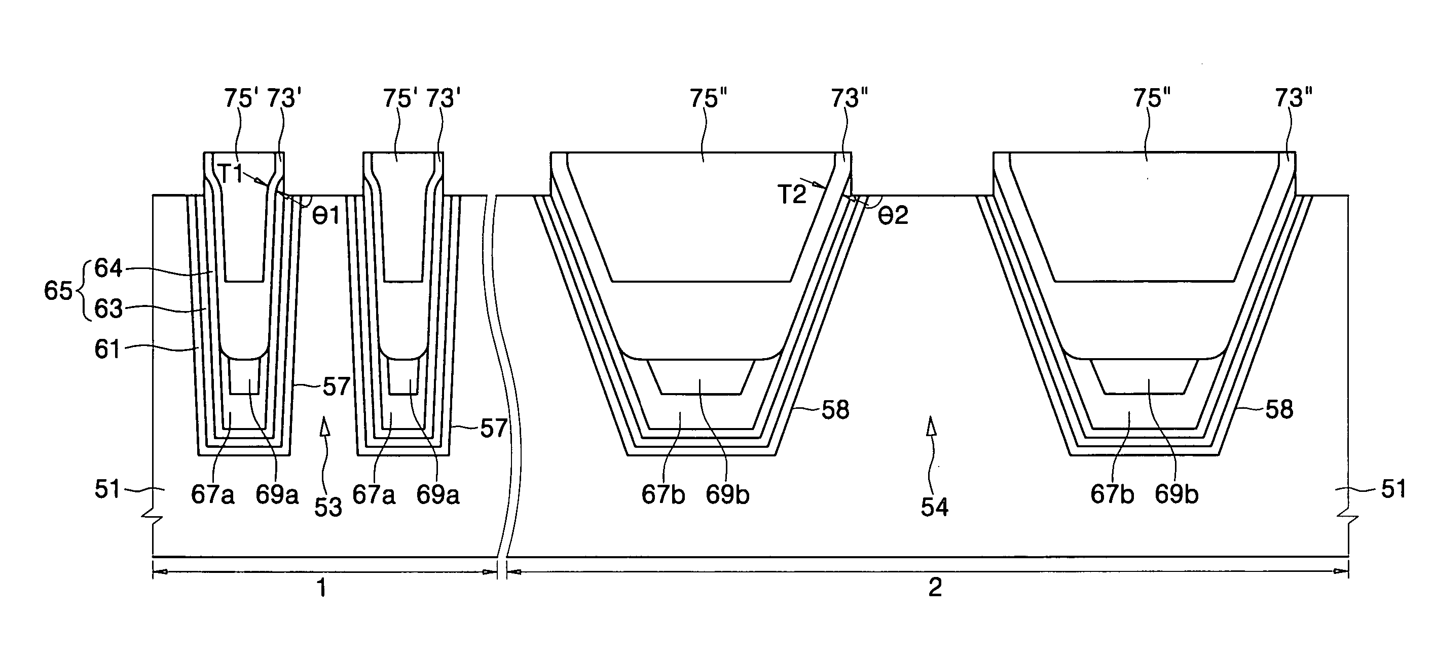
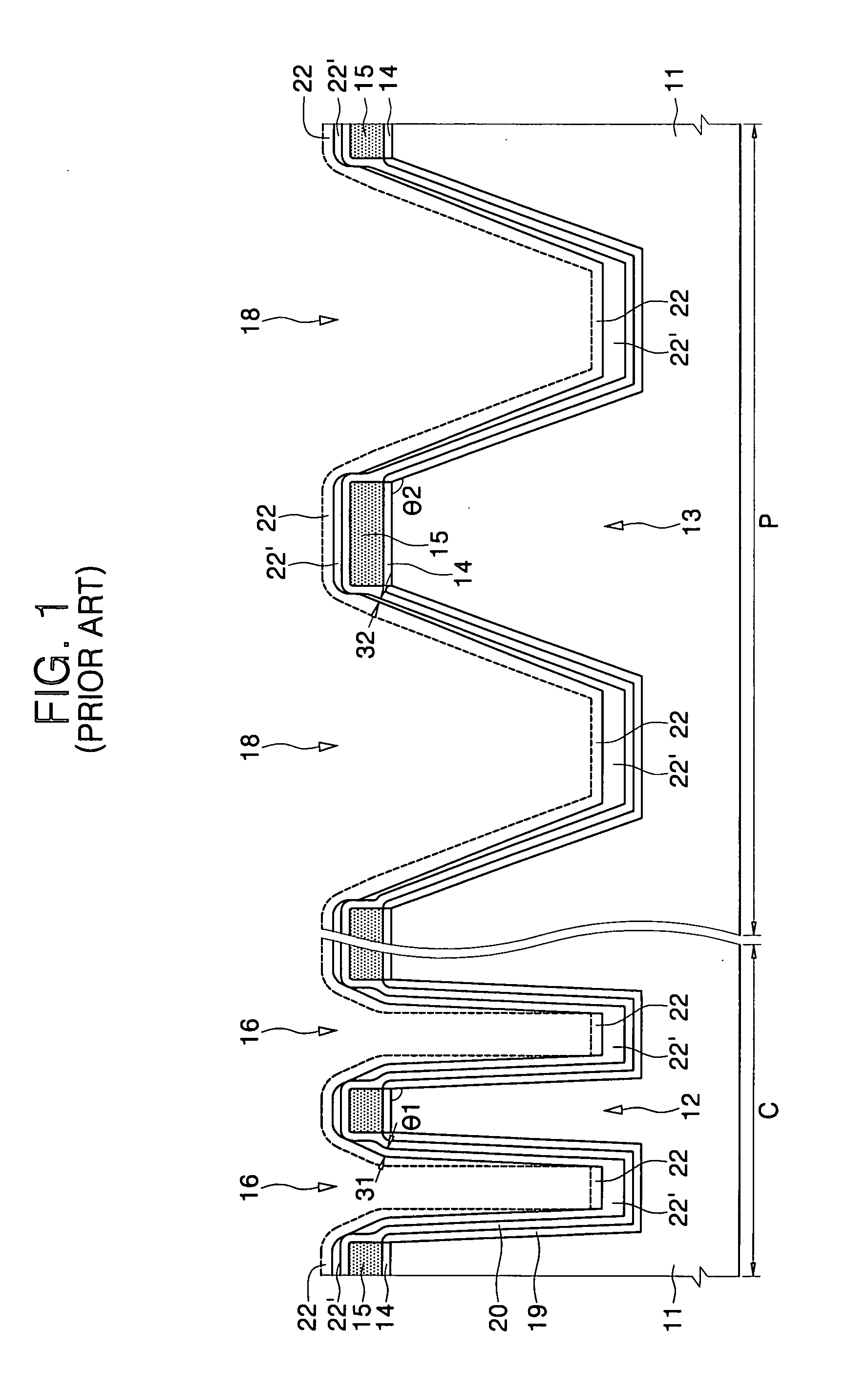
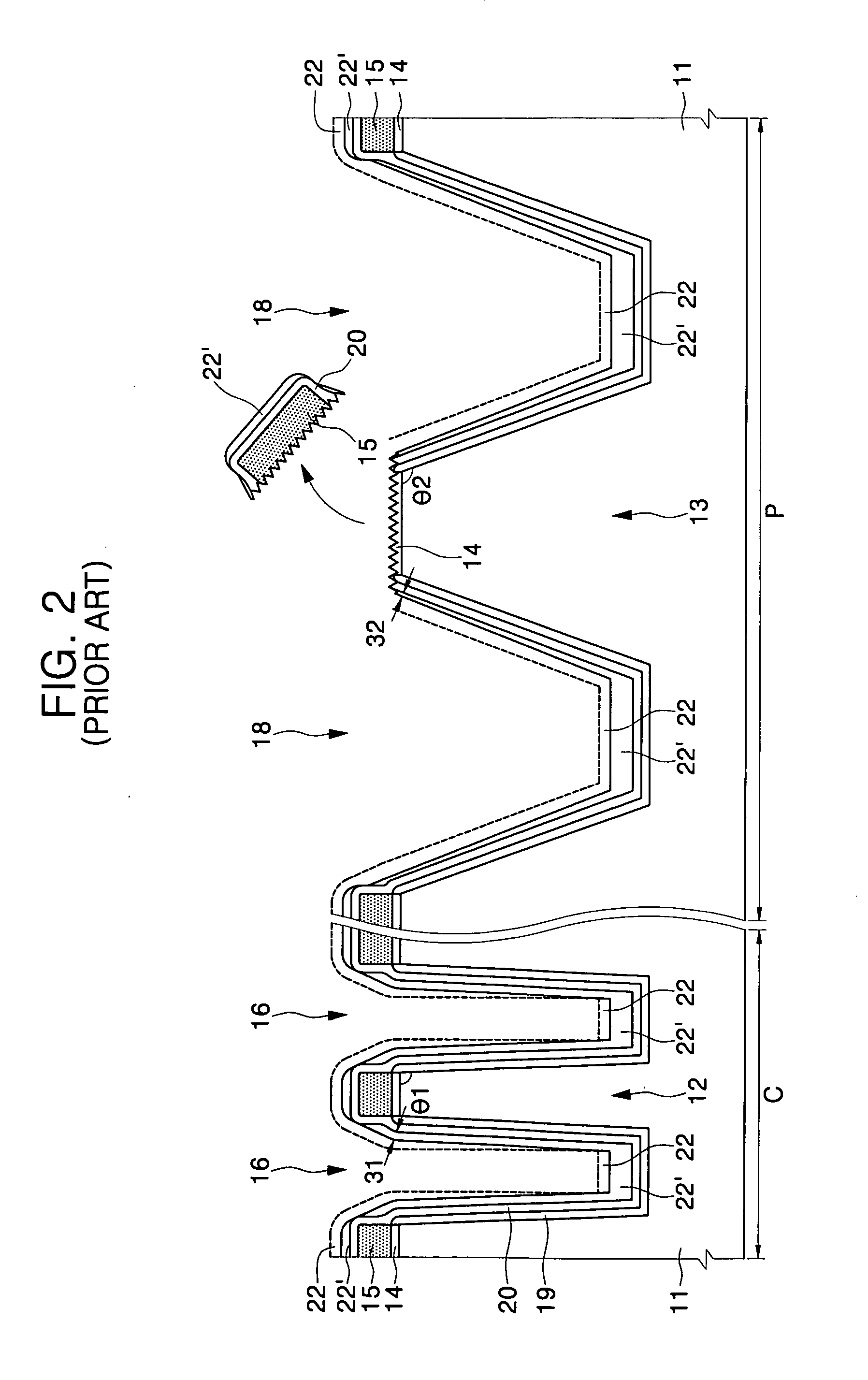
[0027] The invention is described more fully hereinafter with reference to the accompanying drawings, in which embodiments of the invention are shown. This invention may, however, be embodied in many different forms and should not be construed as limited to the embodiments set forth herein. Rather, these embodiments are provided so that this disclosure will be thorough and complete, and will fully convey the scope of the invention to those skilled in the art. In the drawings, the size and relative sizes of layers and regions may be exaggerated for clarity.

[0028] It will be understood that when an element or layer is referred to as being “on”, “connected to” or “coupled to” another element or layer, it can be directly on, connected or coupled to the other element or layer or intervening elements or layers may be present. In contrast, when an element is referred to as being “directly on,”“directly connected to” or “directly coupled to” another element or layer, there are no interveni...


PUM


Abstract

Trench isolation methods include forming a first trench and a second trench, having a larger width than the first trench, in a semiconductor substrate. A lower isolation layer is formed having a first thickness on an upper sidewall of the first trench and a second thickness on an upper sidewall of the second trench using a first high density plasma deposition process, the second thickness being greater than the first thickness. An upper isolation layer is formed on the semiconductor substrate including the lower isolation layer using a second high density plasma deposition process, different from the first high density plasma deposition process. The first and second high density plasma deposition processes may be chemical vapor deposition processes. Semiconductor devices including a trench isolation structure are also provided.

Description

CROSS-REFERENCE TO RELATED APPLICATION [0001] This application is related to and claims priority from Patent Application No. 2005-0084254, filed Sep. 9, 2005, in the Korean Intellectual Property Office, the disclosure of which is hereby incorporated by reference herein in its entirety. BACKGROUND OF THE INVENTION [0002] The present invention relates to semiconductor devices and methods of fabricating the same, and more particularly, to semiconductor devices having a trench isolation structure and methods of fabricating the same. [0003] As semiconductor devices become more highly integrated, an increase in aspect ratio of an isolation trench of the devices is generally required. The increase in aspect ratio typically makes it more difficult to fill the trench with an insulating layer without voids. A high-density plasma chemical vapor deposition (HDPCVD) technique having an excellent gap filling property is known for use in forming trench isolation layers in highly integrated semicon...

Claims


Application Information

Patent Timeline
Patent Type & Authority Applications(United States)
IPC IPC(8): H01L21/76
CPCH01L21/76232H01L21/76229H01L21/02274H01L21/02164H01L21/0214H01L21/0217H01L21/02238H01L21/02211H01L21/31111H01J37/321
Inventor SHIN, DONG-SUKLEE, SEUNG-JINJEONG, YONG-KUKPARK, KI-KWAN
Owner SAMSUNG ELECTRONICS CO LTD
Why Eureka
Try Eureka