
Memory system and method having point-to-point link
a memory system and point-to-point technology, applied in the field of memory systems, can solve problems such as adversely affecting the operation speed of the memory system, and achieve the effects of avoiding increasing the package size of more secondary memories, reducing the difficulty of signal routing, and increasing signal integrity
- Summary
- Abstract
- Description
- Claims
- Application Information
AI Technical Summary
Benefits of technology
Problems solved by technology
Method used
Image

Examples
Embodiment Construction
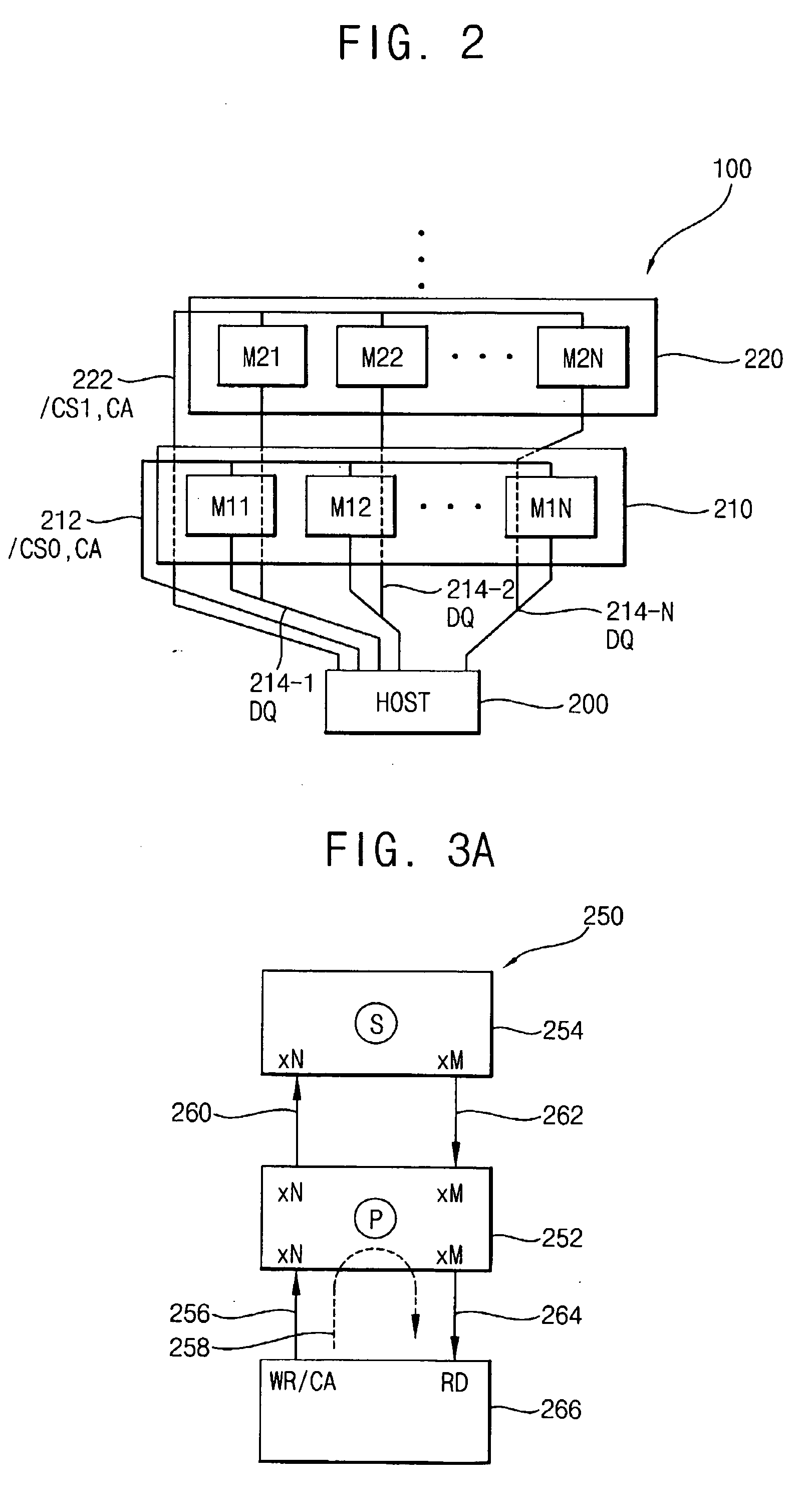
[0054]FIGS. 3A-3C are schematic diagrams functionally illustrating a memory system 250 having a PTP link architecture. The memory system of FIGS. 3A and 3B includes a primary memory device 252 and a secondary memory device 254. A host or controller 266 sends and receives commands and data to and from the primary 252 and secondary 254 memories while executing program instructions.
[0055] The controller 266 includes a write / CA (WR / CA) port through which write data and CA signals can be transferred to the memory devices 252 and 254. The controller 266 also includes a read (RD) port through which data read from the memory devices 252 and 254 are received by the controller 266.
[0056] The primary memory device 252 includes four ports. A first receive port labeled “xN” can include N pins and receives WR / CA signals from the controller 266 on lines 256. A first transmit port labeled “xN” can include N pins and transmits WR / CA signals to the secondary memory 254 along lines 260. A second rec...
PUM
 Abstract
Description
Claims
Application Information