Process for conducting high-speed bitmapping of memory cells during production

a memory cell and high-speed bitmapping technology, applied in the field of high-speed bitmapping of memory cells during production, can solve the problems of large space occupation, memory defects that are very likely to show up in memory areas first, and defects in the di

Inactive Publication Date: 2007-03-15
LSI CORPORATION
View PDF12 Cites 32 Cited by
  • Summary
  • Abstract
  • Description
  • Claims
  • Application Information

AI Technical Summary

Problems solved by technology

Memory requires a high density of active elements (i.e., transistors) and therefore fabrication defects are very likely to show up in memory areas first.
Additionally, in more modem designs, memory is taking up larger and larger portions of the space on each die.
If there is any variance between the data read into the die and the data read out of the die, then there is a defect in the die.
This is a much more difficult and time-consuming process.
Considering that some die can have more than 100 memory instances each having up to a million or more bits or more of memory, this can take some time.
Traditional bitmapping takes a substantial amount of time.
Due to the substantially increased test time and the associate

Method used


Image

  • Process for conducting high-speed bitmapping of memory cells during production
  • Process for conducting high-speed bitmapping of memory cells during production
  • Process for conducting high-speed bitmapping of memory cells during production

Examples


Embodiment Construction

[0023] The present invention has been particularly shown and described with respect to certain embodiments and specific features thereof. The embodiments set forth hereinbelow are to be taken as illustrative rather than limiting. It should be readily apparent to those of ordinary skill in the art that various changes and modifications in form and detail may be made without departing from the spirit and scope of the invention.

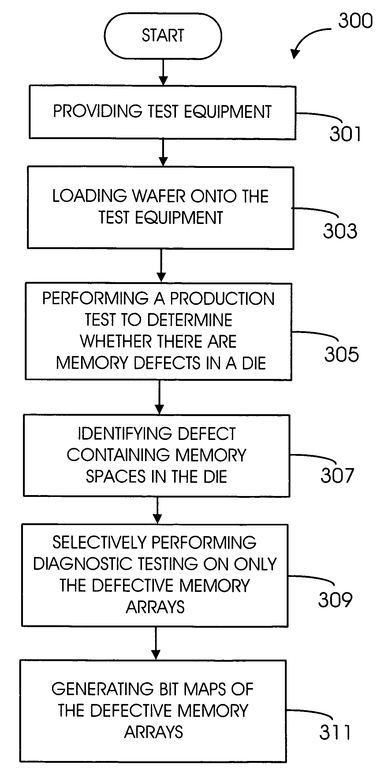
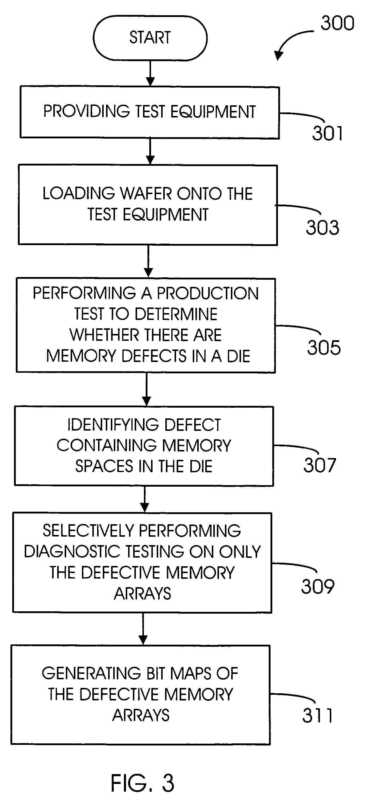
[0024] In general terms the following discussion concerns methods, apparatus, and computer program products for conducting fast bitmapping of memory instances during production. In one general approach, a production test of each die on a semiconductor wafer is performed. The test is intended to be performed on die having a plurality of memory instances supported with built-in self repair (BISR) functions. Such memory repair functionality includes built-in self test (BIST) functions for determining if selected memory instances are defective. So in addition to de...


PUM


Abstract

The present invention is directed to a method of fast bitmapping defective memory arrays in semiconductor integrated circuit dice formed on a wafer. The method involves loading a wafer onto automated test equipment. Initial production testing is then performed on each die of the wafer to determine whether the memory arrays of each die are functioning properly. Where a die is found to have at least one defective memory array, the particular memory arrays of the die that contain defect are specifically identified using BIST circuitry forming part of the die. Then selectively performed diagnostic testing is performed on only the failed memory arrays of each defective die to generate memory array defect data. The memory array defect data is used to generate bit maps of the failed memory arrays using the memory array data.

Description

FIELD OF THE INVENTION [0001] The invention described herein relates generally to methods and processes for conducting fast bit mapping of defective memory locations on semiconductor integrated circuits. Among other things, the technology finds applicability to fast bit mapping of defective memories on semiconductor integrated circuits in both packaged and wafer forms. BACKGROUND OF THE INVENTION [0002] In the semiconductor industry it is common to test integrated circuit (IC) devices during fabrication to insure that they are functional. Currently a wide variety of testing processes are used to conduct such testing. The invention disclosed herein introduces improved methods and apparatus for testing such IC devices. [0003] As is known to those having ordinary skill in the art IC's are manufactured on semiconductor wafers (typically formed of silicon or other semi-conducting substrates). A number of IC devices are formed on each wafer with the number of IC devices formed being a fac...

Claims


Application Information

Patent Timeline
IPC IPC(8): G11C29/00
CPCG11C29/006G11C2029/5604G11C29/56
Inventor WARD, MARK A.CONDER, JEFF EARL
Owner LSI CORPORATION
Why Eureka
Try Eureka