

Coil and coil support for generating a plasma
a coil and plasma technology, applied in the field of plasma generators, can solve the problems of contaminating the product, affecting the production efficiency of the product, and the inability to achieve the desired effect of reducing the generation of particulates
- Summary
- Abstract
- Description
- Claims
- Application Information
AI Technical Summary
Benefits of technology
Problems solved by technology
Method used
Image

Examples
Embodiment Construction
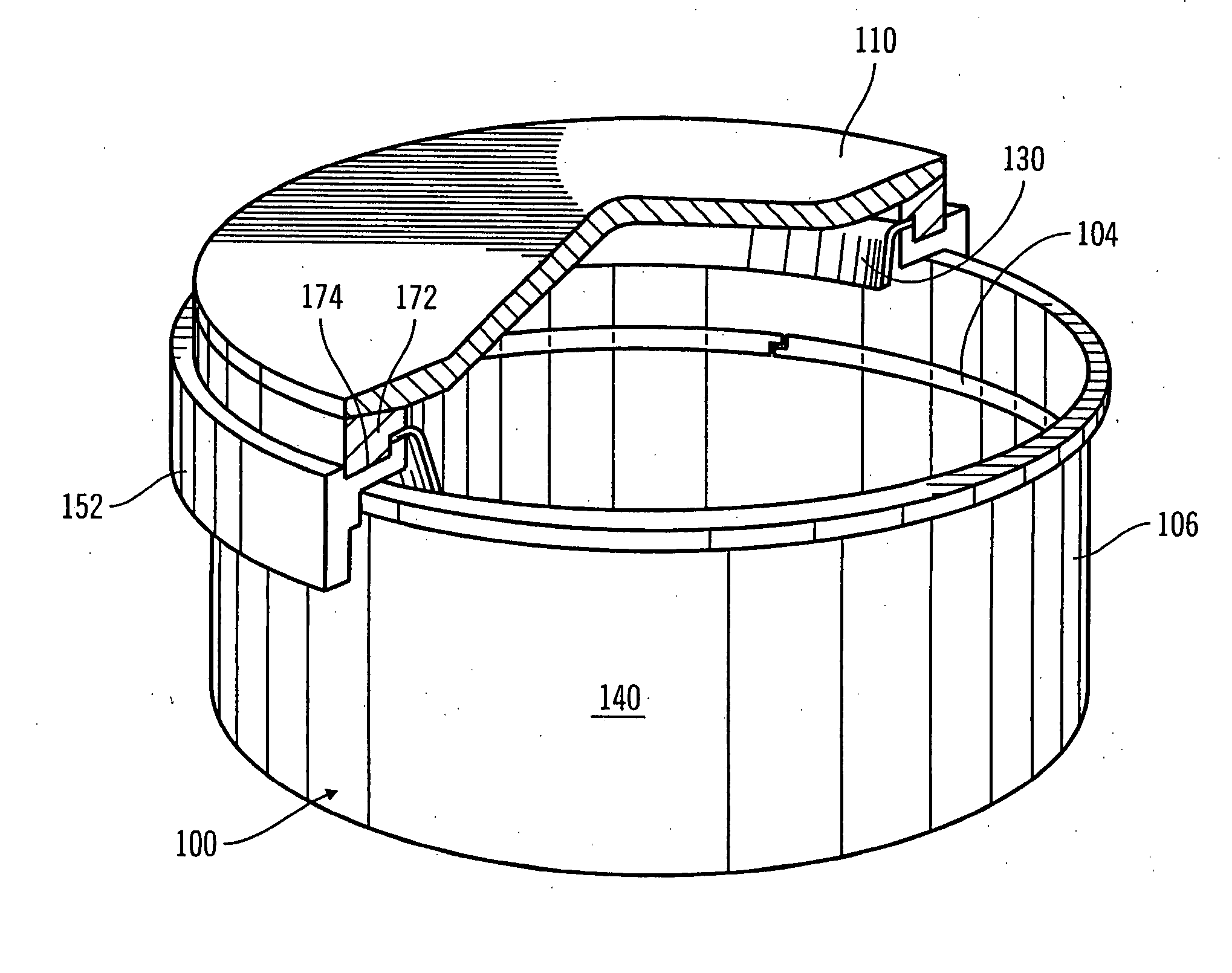
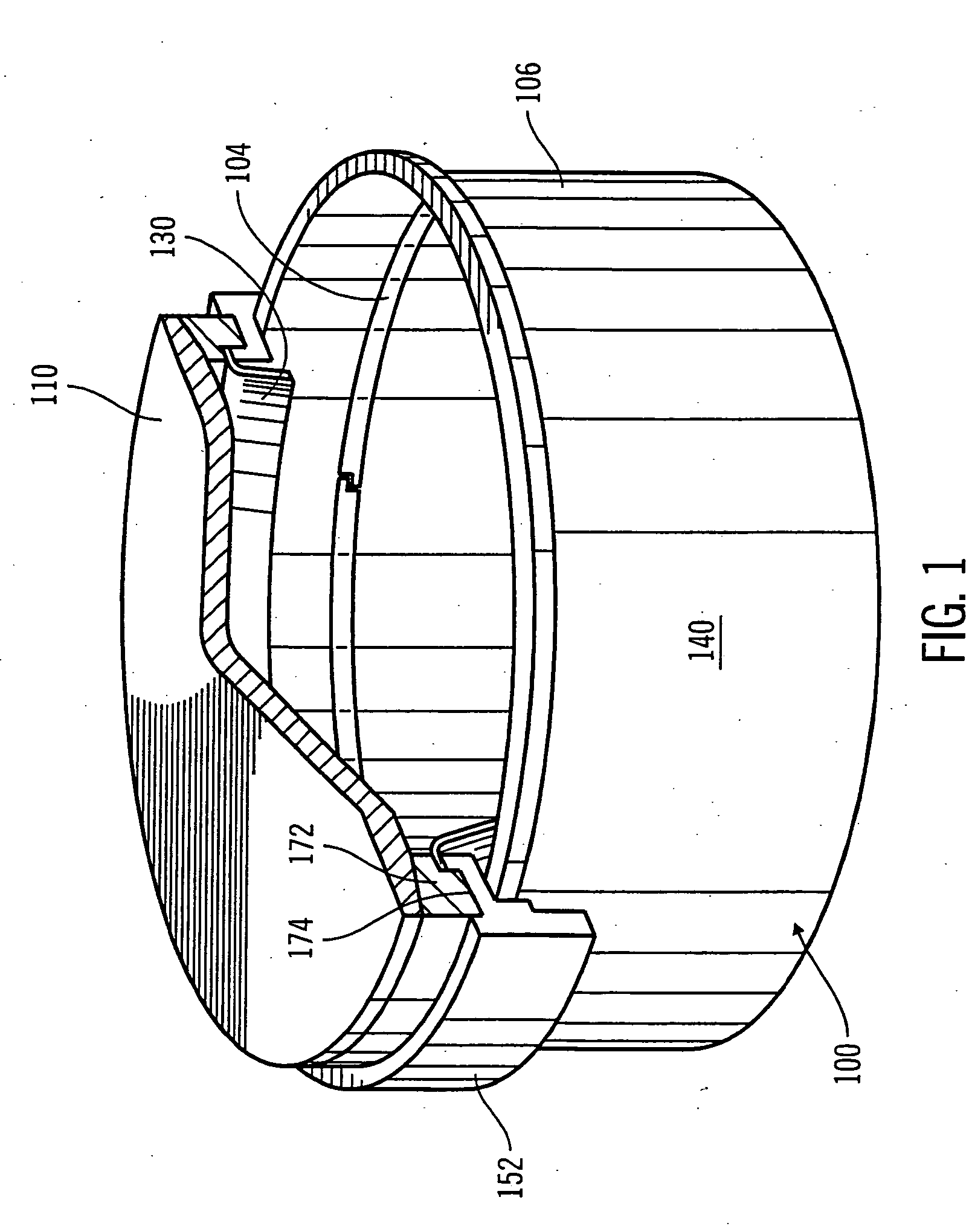
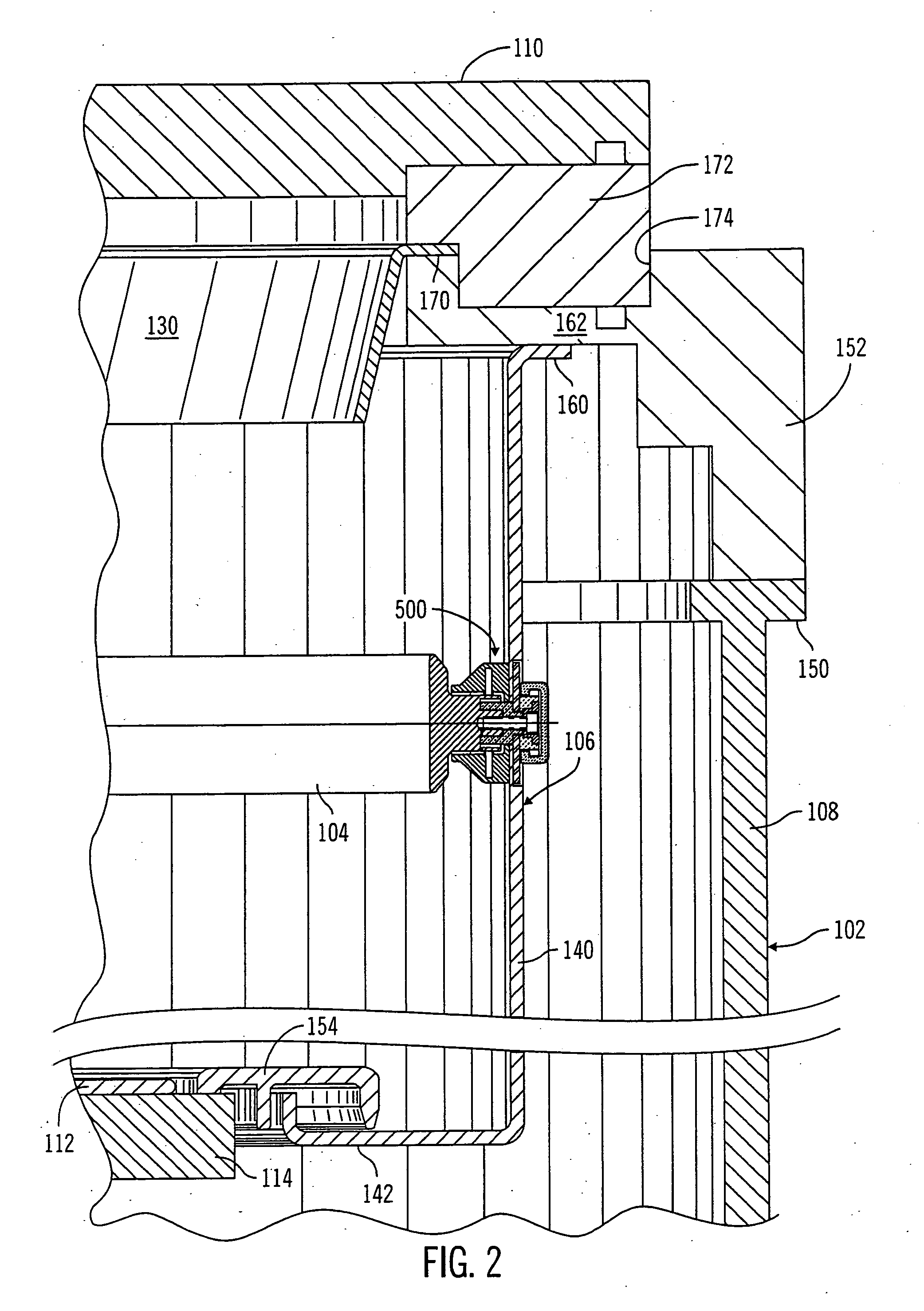
[0006] In accordance with one aspect of the invention, a coil is carried internally in a semiconductor fabrication chamber by a plurality of novel coil standoffs and RF feedthrough standoffs which reduce generation of particulates. In the illustrated embodiment, the coil has an outer face facing a shield wall, in which the outer face defines a fastener recess extending partially through the coil. A standoff includes a fastener member adapted to fasten the coil to the shield wall. The coil outer face fastener recess is adapted to receive the fastener member. As explained below, such an arrangement can reduce the generation of particulates by the coil and the coil standoffs.
[0007] There are additional aspects to the present inventions as discussed below. It should therefore be understood that the preceding is merely a brief summary of one embodiment of the present inventions. It should further be understood that numerous changes to the disclosed embodiments can be made without depart...
PUM
| Property | Measurement | Unit |
|---|---|---|
| DC power | aaaaa | aaaaa |
| RF power | aaaaa | aaaaa |
| width | aaaaa | aaaaa |
Abstract
Description
Claims
Application Information