Method and apparatus for providing wafer centering on a track lithography tool

a technology of lithography tool and track, which is applied in the direction of instrumentation, electric programme control, program control, etc., can solve problems such as damage or breakage of wafers, and achieve the effects of reducing particle generation and defect risk, improving wafer handling reliability, and reducing contact with substra

Inactive Publication Date: 2009-04-30
SOKUDO CO LTD
View PDF2 Cites 17 Cited by
  • Summary
  • Abstract
  • Description
  • Claims
  • Application Information

AI Technical Summary

Benefits of technology

[0011]Many benefits are achieved by way of the present invention over conventional techniques. For example, embodiments of the present invention allow for improved wafer handling reliability and reduced contact with the substrate, thus reducing particle generation and the risk of defects. Additional embodiments of the present invention provide reduced risk of wafer breakage or chipping, and wafer breakage can be detected at an early stage reducing the potential impact of an adverse event. Furthermore, embodiments of the present invention provide accurate placements that can help to protect expensive components used within the chamber from damage from the wafer, and can ensure proper placement even with a small placement area. Depending upon the embodiment, one or more of these benefits, as well as other benefits, may be achieved. These and other benefits will be described in more detail throughout the present specification and more particularly below in conjunction with the following drawings.

Problems solved by technology

If a wafer is incorrectly positioned during placement within the processing chamber, it can result in uneven processing of the wafer in different regions or even cause breakage or damage to the wafer.

Method used


Image

  • Method and apparatus for providing wafer centering on a track lithography tool
  • Method and apparatus for providing wafer centering on a track lithography tool
  • Method and apparatus for providing wafer centering on a track lithography tool

Examples


Embodiment Construction

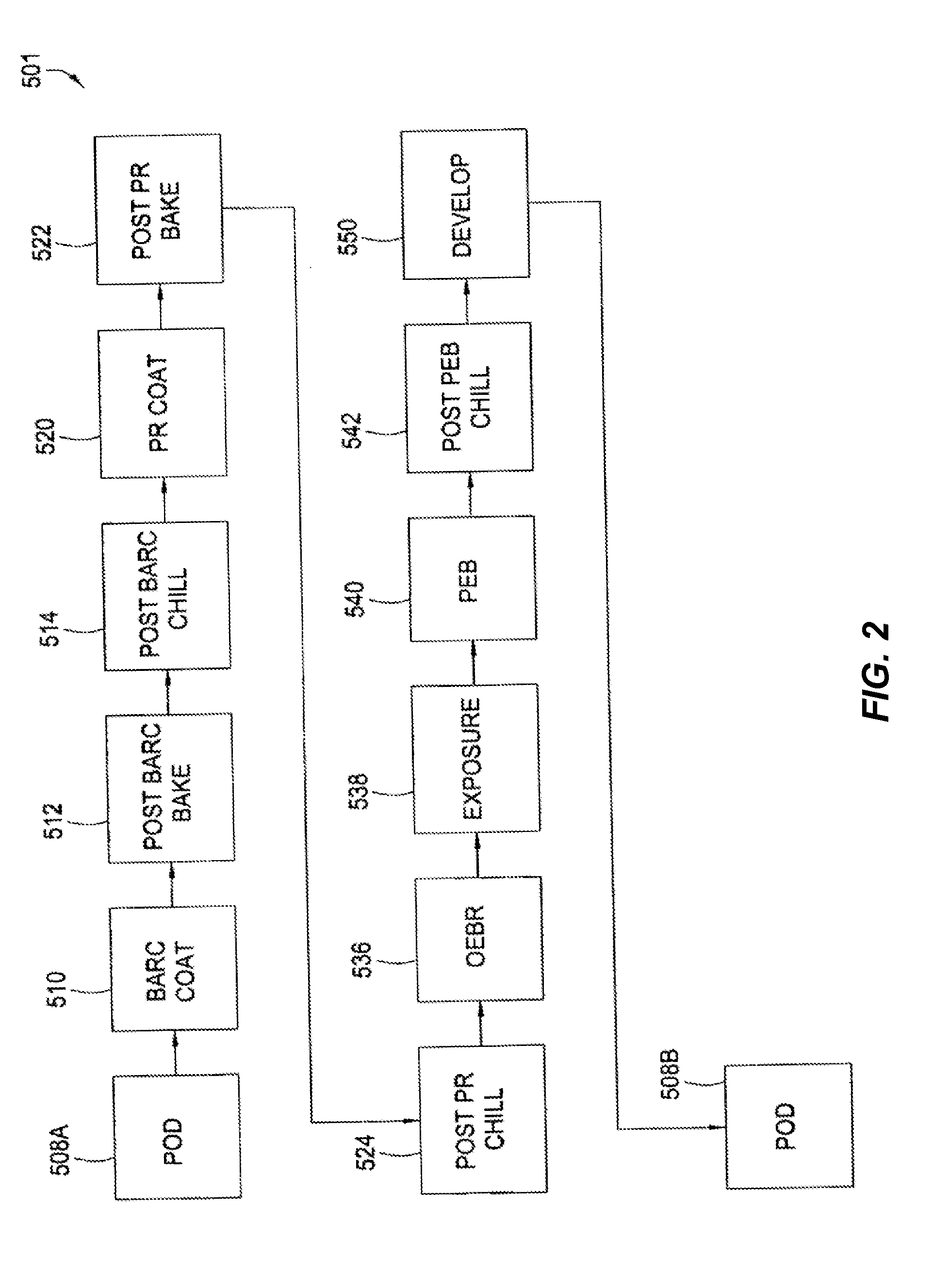
[0018]According to the present invention, methods and systems related to the field of substrate processing equipment are provided. More particularly, embodiments of the present invention pertain to a method and system for accurately centering a substrate within a semiconductor processing system. While embodiments of the invention may prove to be particularly useful in a track lithography tool, other embodiments of the invention can be used in other applications where it is desirable to accurately position a substrate to be processed.

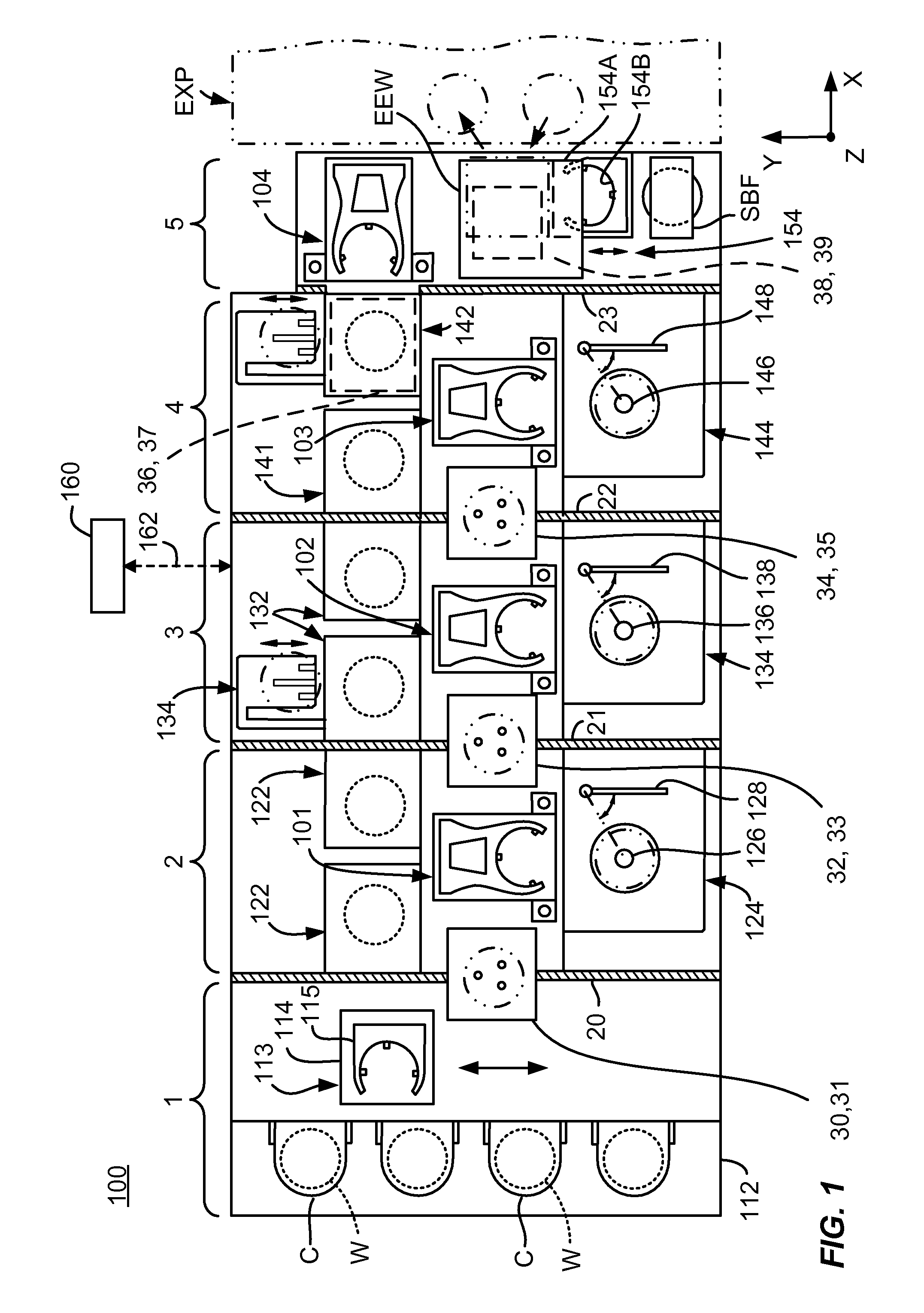
[0019]FIG. 1 is a plan view of a track lithography tool according to an embodiment of the present invention. In the embodiment illustrated in FIG. 1, the track lithography tool is coupled to an immersion scanner. An XYZ rectangular coordinate system in which an XY plane is defined as the horizontal plane and a Z axis is defined to extend in the vertical direction is additionally shown in FIG. 1 for purposes of clarifying the directional relationship ther...


PUM


Abstract

An apparatus for centering a substrate in a track lithography tool includes a processing chamber having an opening large enough to admit the substrate. The processing chamber includes a substrate support member. The substrate is characterized by a diameter and comprises a mounting surface, a process surface, and an edge. The apparatus also includes a clamped robot blade including a substrate support surface adapted to support the mounting surface of the substrate, two edge contact regions, and a base contact region. The clamped robot blade also includes a clamping system adapted to move at least one of the two edge contact regions or the base contact region from an unclamped position to a clamped position, thereby making contact between the edge of the substrate and the two edge contact regions and the base contact region in the clamped position. The apparatus further includes a robot arm coupled to the clamped robot blade.

Description

BACKGROUND OF THE INVENTION[0001]The present invention relates generally to the field of substrate processing equipment. More particularly, the present invention relates to a method and apparatus for performing wafer centering on a track lithography tool. Merely by way of example, the method and apparatus of the present invention utilize an wafer position correction system with a clamped robot blade to prevent misalignment of a substrate upon the robot blade. The method and system can be applied to other semiconductor processing chambers commonly used in semiconductor processing equipment.[0002]Modern integrated circuits contain millions of individual elements that are formed by patterning the materials that make up the integrated circuit, such as silicon, metal and / or dielectric layers, to sizes that are small fractions of a micrometer. One of the techniques used throughout the industry for forming such patterns is photolithography. A typical photolithography process sequence gener...

Claims


Application Information

Patent Timeline
Patent Type & Authority Applications(United States)
IPC IPC(8): H01L21/68B25J15/00B65G29/00G05B19/18H01L21/02
CPCH01L21/67225Y10T74/20317H01L21/68707H01L21/68
Inventor SALEK, MOHSEN S.
Owner SOKUDO CO LTD
Why Eureka
Try Eureka