Substrate for semiconductor device and semiconductor device

a technology for semiconductor devices and substrates, which is applied in the direction of printed circuit components, printed circuit non-printed electric components association, printed circuit manufacturing, etc., can solve the problems of difficult flattening of the top part of the implanted capacitor, the capacitor cannot meet the speeding up ics, and the substrate cannot be suitable for mounting capacitors having enough capacity on the substrate, etc., to achieve superior electric characteristics to high-speed signals, reduce circuit inductance, and effectively short circuit lengths

Inactive Publication Date: 2007-03-22
NIPPON MICRON
View PDF6 Cites 3 Cited by
  • Summary
  • Abstract
  • Description
  • Claims
  • Application Information

AI Technical Summary

Benefits of technology

[0011] Thus, the present invention was conceived to solve the above described problems, and an object of the present invention is to provide a substrate for a semiconductor device and a semiconductor device, which are capable of highly shortening a cable length between a working part of a semiconductor element and a circuit component, e.g., decoupling capacitor, so as to effectively reduce circuit inductance, corresponding to further speed-up of semiconductor elements by facilitating the mounting of the circuit component, e.g., decoupling capacitor, fabricated separately from the substrate and being mass-produced.
[0014] In the substrate, the substrate may be constituted by a core plate and a cable layer or layers formed on the core plate, and the surface of the substrate, which is opposite to the element mounting surface thereof, may be counterbored so as to form a component mounting hole where a connection terminal, which is formed in the cable layer, is exposed in the inner bottom face. With the element mounting hole formed by counterboring the substrate, the circuit component can be mounted by effectively using thickness of the substrate, so that the circuit component, e.g., decoupling capacitor having large capacity, can be easily mounted and superior electric characteristics to high-speed signals can be gained.
[0015] In the substrate, the component mounting hole may be located in a semiconductor element mounting area; a cable length between the semiconductor element and the circuit component can be effectively shortened, so that electric characteristics to high-speed signals can be improved.
[0017] Further, the semiconductor element may be mounted on the substrate by flip-chip connection. Since the semiconductor element is mounted on the substrate by flip-chip connection, the cable length between the semiconductor element and the circuit component can be effectively shortened; therefore, circuit inductance can be reduced, and the semiconductor device having superior electric characteristics to high-speed signals can be produced.

Problems solved by technology

However, in the case of forming the decoupling capacitor in, for example, a build-up layer, the capacity must be 1 / 10,000-1 / 10 of that of the substrate in which the capacitor is set, so the substrate cannot suitably meet the speeding up ICs.
In case of mounting circuit components on the surface opposite to the semiconductor element mounting surface, the circuit components must be lower than solder bumps, so only the thin circuit components can be mounted; namely it is difficult to mount the capacitor having enough capacity on the substrate.
A capacitor may be implanted near the surface of the substrate and a cable layer or layers may be formed thereon by the build-up process, but it is difficult to flatten a top part of the implanted capacitor; therefore a thick capacitor cannot be implanted, and enough capacity cannot be gained.
Further, thermal stress working between the semiconductor element, the substrate and the capacitor lower reliability of connected parts thereof.
Thus, it is difficult to apply this method to mass-producing the substrates of semiconductor devices.

Method used


Image

  • Substrate for semiconductor device and semiconductor device
  • Substrate for semiconductor device and semiconductor device
  • Substrate for semiconductor device and semiconductor device

Examples


Embodiment Construction

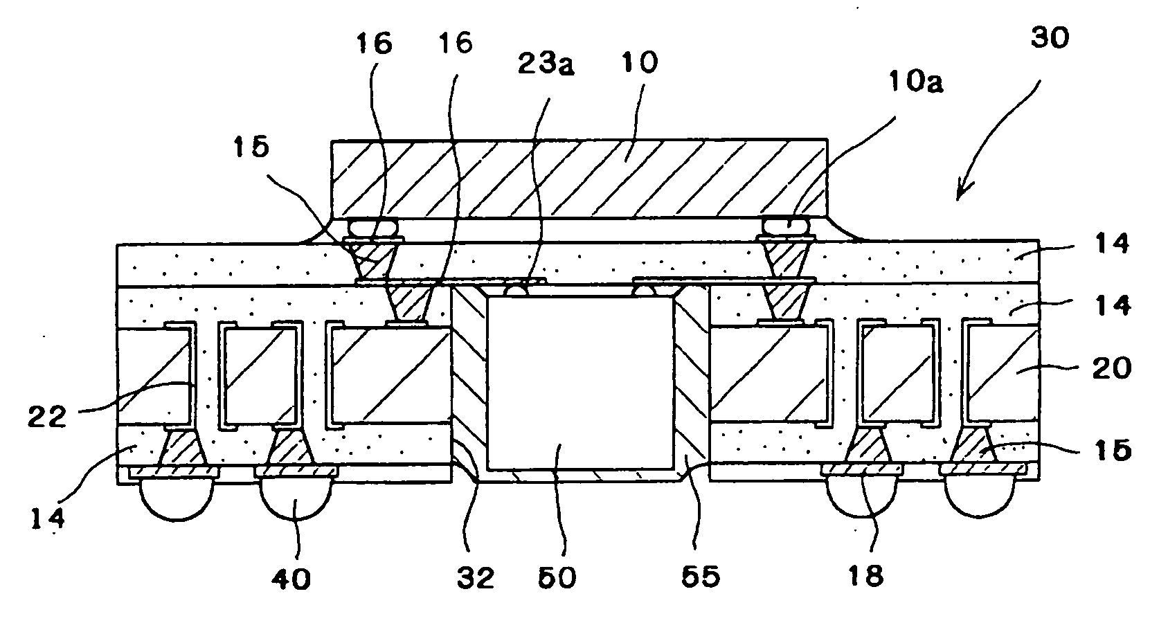
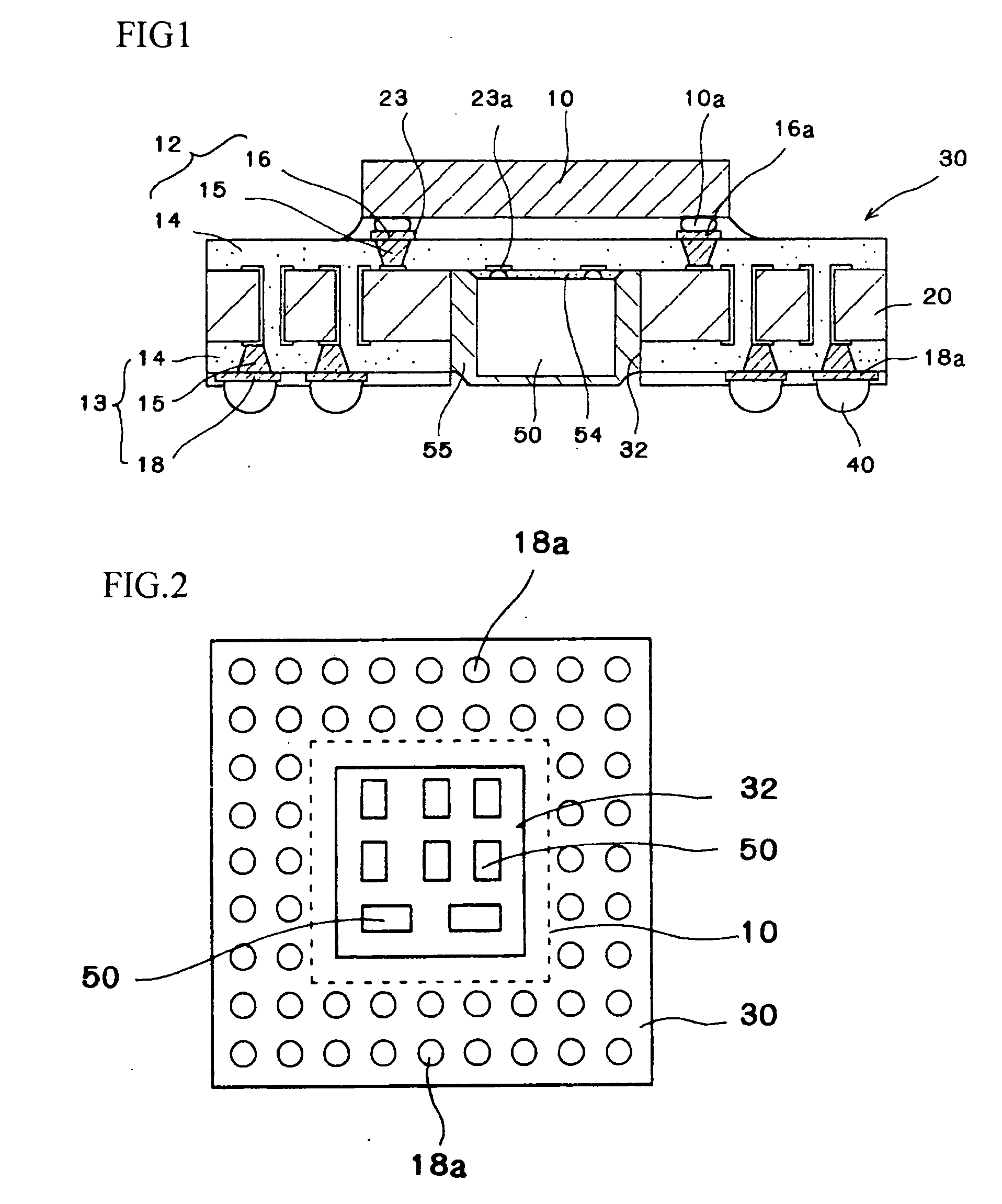
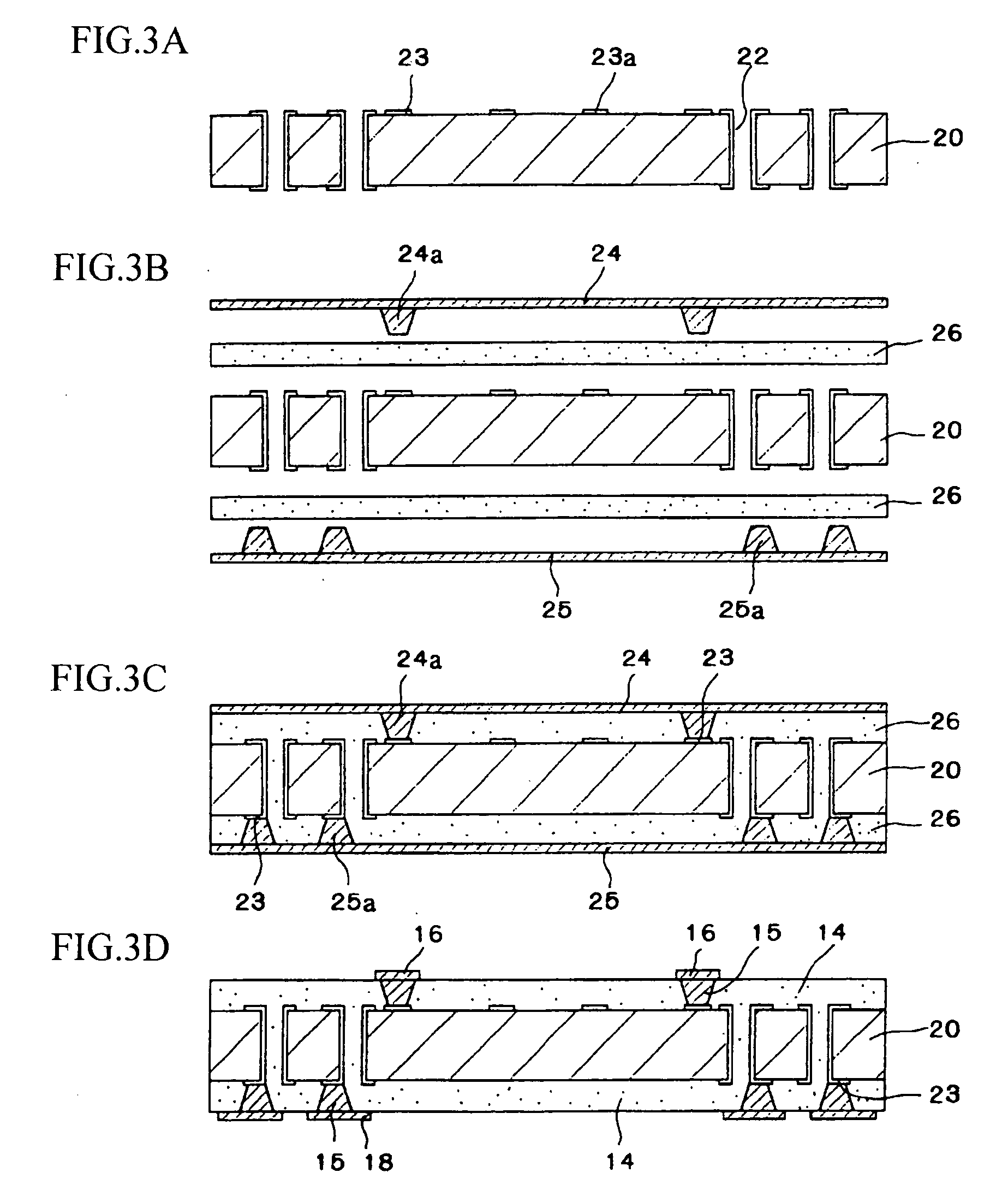
[0024] Preferred embodiments of the present invention will now be described in detail with reference to the accompanying drawings. FIG. 1 is a sectional view of a semiconductor device, in which a semiconductor element 10 is mounted on a substrate 30 of the present invention by flip-chip connection.

[0025] Circuit components 50, e.g., decoupling capacitor, fabricated separately from the substrate 30 are mounted on the substrate, a surface opposite to a semiconductor element mounting surface is counterbored so as to form a component mounting hole 32, and the circuit components 50 are accommodated in the component mounting hole 32.

[0026] The component mounting hole 32 is formed by counterboring the substrate, it is a concave capable of accommodating one or a plurality of the circuit components 50, connection terminals 23a, which are electrically connected to the semiconductor element 10, are exposed in an inner bottom face of the component mounting hole, and the connection terminals 2...


PUM


Abstract

The present invention provides to a substrate for a semiconductor device, in which electric characteristics to high-speed signals are enhanced by facilitating the mounting of a circuit component, such as a decoupling capacitor, fabricated separately from the substrate. The substrate (30) for a semiconductor device, on which the circuit component (50), such as a decoupling capacitor, can be mounted, is counterbored from the mounting surface side thereof, and a component mounting hole (32) where a connection terminal (23a), which will be electrically connected to the circuit component (50), is exposed in the inner bottom face is made by counterboring. The circuit component (50) is mounted and electrically connected to the connection terminal (23a), and a semiconductor element (10) is mounted on the substrate by flip-chip connection.

Description

[0001] This application is a Divisional of co-pending application Ser. No. 10 / 560,938 filed on Dec. 15, 2005 and for which priority is claimed under 35 U.S.C. § 120. application Ser. No. 10 / 560,938 is the national phase of PCT International Application No. PCT / JP2004 / 008431 filed on Jun. 16, 2004 under 35 U.S.C. § 371, and this application claims priority to application Ser. No. 2003-170852 filed on Jun. 16, 2003 in Japan under 35 U.S.C § 119. The entire contents of each of the above-identified applications are hereby incorporated by reference.FIELD OF TECHNOLOGY [0002] The present invention relates to a substrate for a semiconductor device and a semiconductor device, more precisely relates to a substrate for a semiconductor device, on which a circuit component, such as a decoupling capacitor, can be easily mounted, and a semiconductor device having the substrate. BACKGROUND TECHNOLOGY [0003] With faster ICs, a variation of electric current working therethrough must be great, and a ...

Claims


Application Information

Patent Timeline
Patent Type & Authority Applications(United States)
IPC IPC(8): H01L23/48H01L21/48H01L21/56H01L21/60H01L23/13H01L23/24H01L23/498H01L23/50H01L25/00H05K1/02H05K1/18H05K3/00H05K3/46
CPCH01L21/486H05K2201/10674H01L23/13H01L23/24H01L23/49816H01L23/50H01L2224/16H01L2924/01078H01L2924/15311H01L2924/1532H01L2924/19106H01L2924/3025H05K1/183H05K3/0044H05K3/4602H05K3/4652H05K3/4697H01L21/563H01L2924/00011H01L2924/00014H01L2224/0401
Inventor KOMATSU, RYUJI
Owner NIPPON MICRON
Why Eureka
Try Eureka