Liquid crystal display device

a display device and liquid crystal technology, applied in semiconductor devices, instruments, optics, etc., can solve the problem of providing superior display characteristics, and achieve the effect of superior display characteristics

Inactive Publication Date: 2007-03-22
SHARP KK
View PDF6 Cites 99 Cited by
  • Summary
  • Abstract
  • Description
  • Claims
  • Application Information

AI Technical Summary

Benefits of technology

[0022] The invention can realize a liquid crystal display device capable of providing superior display characteristics.

Problems solved by technology

As described above, conventional liquid crystal display devices that employ the capacitive coupling HT technique have a problem that they cannot provide superior display characteristics because of occurrence of the burn-in phenomenon though their viewing angle characteristic is improved.

Method used


Image

  • Liquid crystal display device
  • Liquid crystal display device
  • Liquid crystal display device

Examples


example 1

[0081] A liquid crystal display device according to Example 1 of the embodiment of the invention will be described. FIG. 14 schematically shows the configuration of the liquid crystal display device according to the embodiment. As shown in FIG. 14, the liquid crystal display device has the TFT substrate 2, the counter substrate 4, and the liquid crystal layer 6 (not shown in FIG. 14) which is sealed between the two substrates 2 and 4.

[0082] A gate bus line driving circuit 80 incorporating a driver IC for driving the plural gate bus lines and a drain bus line driving circuit 82 incorporating a driver IC for driving the plural drain bus lines are connected to the TFT substrate 2. The driving circuits 80 and 82 output scanning signals and data signals to prescribed gate bus lines and drain bus lines on the basis of prescribed signals that are output from a control circuit 84. A polarizing plate 87 is disposed on that surface of the TFT substrate 2 which is opposite to its TFT elements...

example 2

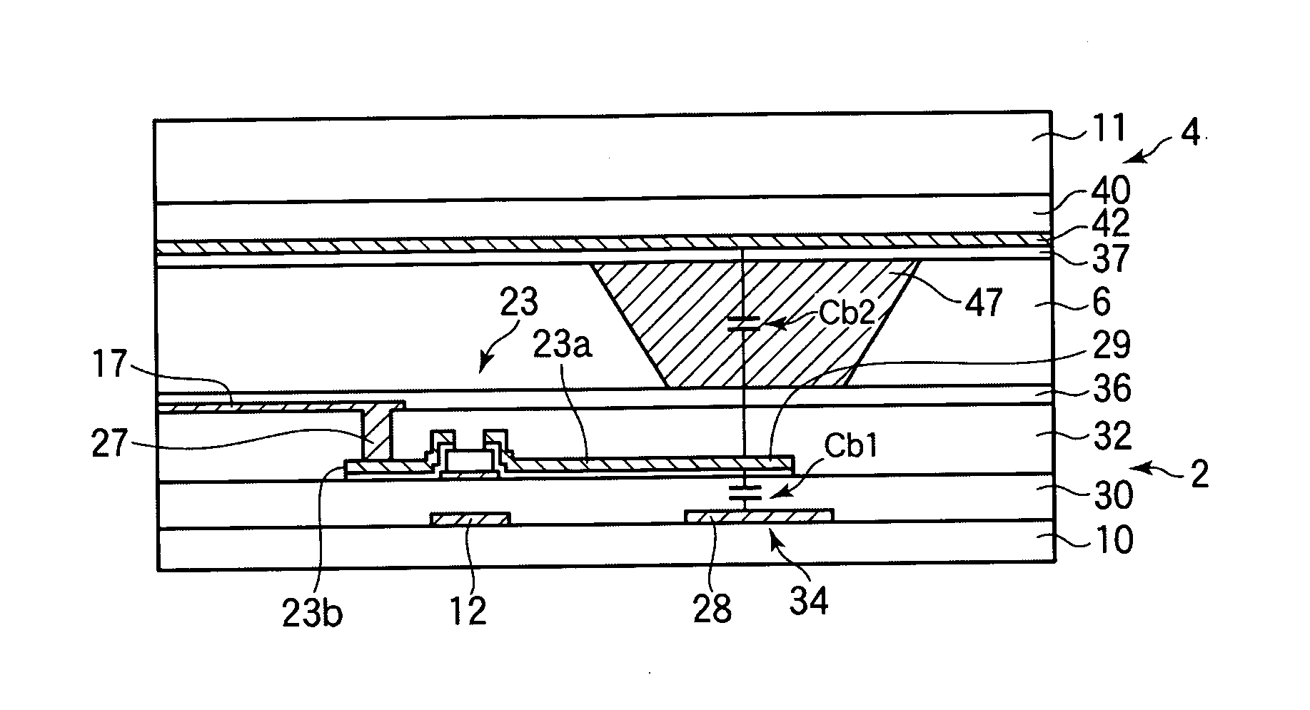
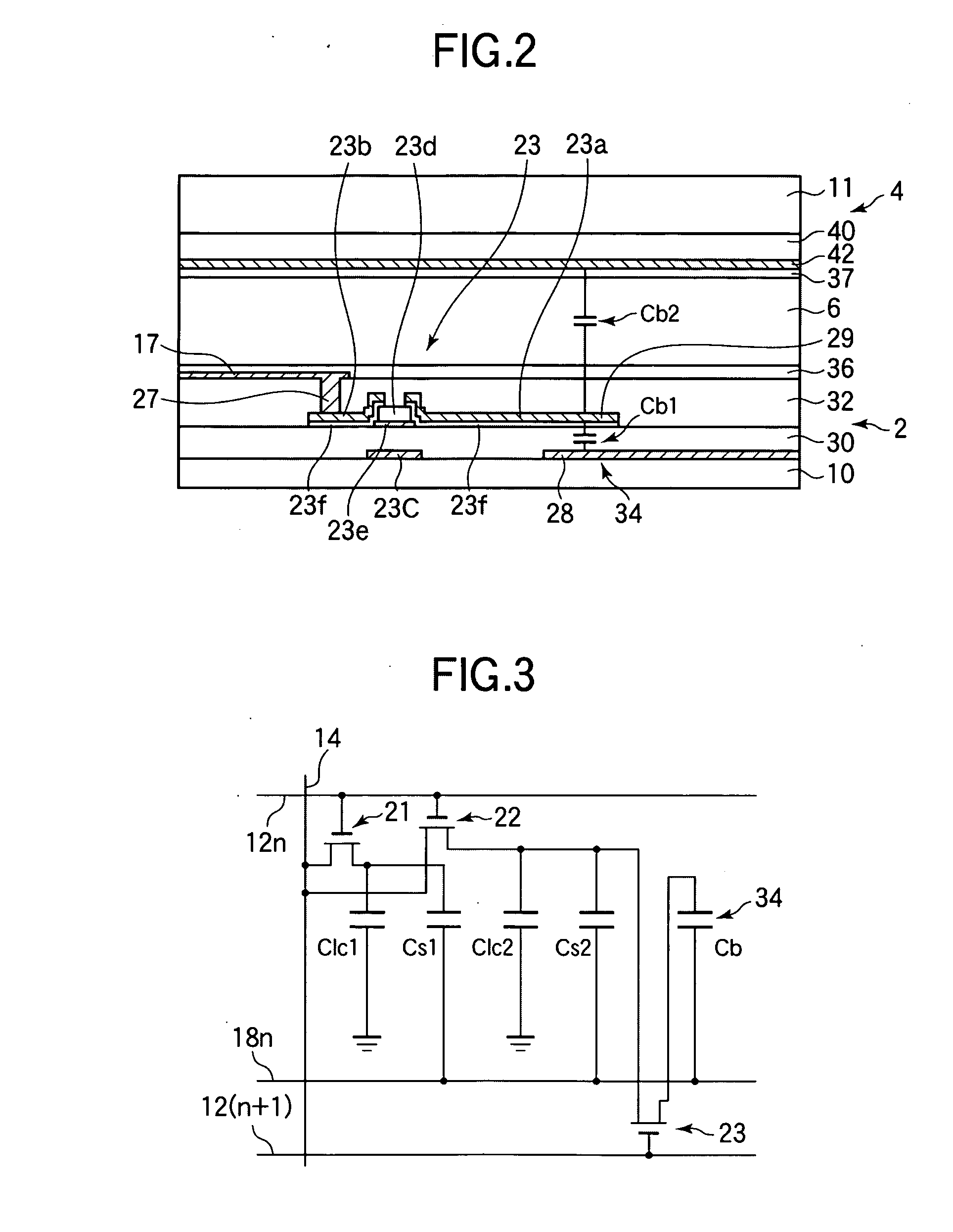
[0087] A liquid crystal display device according to Example 2 of the embodiment will be described. In Example 2, as already shown in FIG. 9, the column-shaped spacer 47 is disposed in the region of formation of the buffer capacitance portion 34. The permittivity e of a liquid crystal varies depending on the alignment state and the voltage application state and hence is a factor of variation of the buffer capacitance Cb (Cb2). In contrast, in Example 2, the capacitance Cb2 is stable because that part of the liquid crystal which is located in the buffer capacitance portion 34 is removed by the column-shaped spacer 47. Incidentally, the buffer capacitance electrodes 28 and 29 of the buffer capacitance portion 34 are usually made of an opaque metal. Therefore, the region of formation of the buffer capacitance portion 34 does not contribute to display and hence is a factor of reduction of the aperture ratio. Example 2 provides an additional advantage that the degree of reduction of the a...

example 3

[0090] In Example 3, according to the fourth principle shown in FIGS. 11A and 11B, the buffer capacitor Cb is formed by the buffer capacitance electrode 61 which is formed in the same layer as the pixel electrodes 16 and 17 and is electrically connected to the connection electrode 35 and the storage capacitance bus line 18 via the contact hole 54, the buffer capacitance electrode 29 which coextends with part of the buffer capacitance electrode 61 and extends from the drain electrode 23a of the TFT 23, and that part of the protective film 32 which is interposed between them. Since the thickness of the protective film 32 can be changed more easily than that of the insulating film 30, in Example 3 the thicknesses of the insulating film 30 and the protective film 32 were set at 350 nm and 150 nm, respectively. With these settings, a buffer capacitance Cb which was 2.3 (350 / 150) times larger than in the case where the insulating film 30 was used as a dielectric layer was obtained in the ...


PUM

PropertyMeasurementUnit
voltagesaaaaaaaaaa
polar angleaaaaaaaaaa
timeaaaaaaaaaa

Abstract

The invention relates to a liquid crystal display device and provides a liquid crystal display device which can achieve high display quality. A liquid crystal display device is provided with first and second TFTs each having a gate electrode connected to an nth gate bus line and a drain electrode connected to a drain bus line; a first pixel electrode connected to a source electrode of the first TFT; a second pixel electrode connected to a source electrode of the second TFT; a third TFT having a gate electrode connected to an (n+1)th gate bus line and a source electrode connected to the second pixel electrode; and a buffer capacitance portion having a buffer capacitance electrode which is formed in the same layer as the first and second pixel electrodes and is connected to a drain electrode of the third TFT and a buffer capacitance electrode connected to a storage capacitance bus line. The buffer capacitance portion establishes capacitive coupling between the drain electrode of the third TFT and the storage capacitance bus line.

Description

BACKGROUND OF THE INVENTION [0001] 1. Field of the Invention [0002] The present invention relates to a liquid crystal display device used as, for example, a display unit of an electronic apparatus. [0003] 2. Description of the Related Art [0004] In recent years, liquid crystal display devices have come to be used for TV receivers, monitor devices of personal computers, etc. In these purposes, liquid crystal display devices are required to have a good viewing angle characteristic that the display screen is viewable from all directions. FIG. 20 is a graph showing transmittance vs. application voltage characteristics (T-V characteristics) of a VA (vertically aligned)-mode liquid crystal display device. The horizontal axis represents the voltage (V) applied to the liquid crystal layer and the vertical axis represents the light transmittance. Line A is a T-V characteristic obtained in the direction perpendicular to the display screen (hereinafter referred to as “front direction”), and li...

Claims


Application Information

Patent Timeline
Patent Type & Authority Applications(United States)
IPC IPC(8): G02F1/1343
CPCH01L27/1255G02F1/136213
Inventor TASAKA, YASUTOSHINAKANISHI, YOHEISHIBASAKI, MASAKAZUKAMADA, TSUYOSHIYOSHIDA, HIDEFUMITSUDA, HIDEAKI
Owner SHARP KK
Why Eureka
Try Eureka