Circuit board and manufacturing method of the circuit board

a manufacturing method and circuit board technology, applied in the field of circuit board and manufacturing method of circuit board, can solve the problems of inability to respond to the demand of miniaturization of circuit board, inability to use the hitherto used technique, etc., and achieve excellent adhesion of plating deposition film and base pattern, high precision, and mechanical strength.

Inactive Publication Date: 2007-03-22
KK TOSHIBA
View PDF6 Cites 25 Cited by
  • Summary
  • Abstract
  • Description
  • Claims
  • Application Information

AI Technical Summary

Benefits of technology

[0010] It is an object of the present invention to provide a circuit board with a fine pitch pattern formed with high precision, excellent in adhesion of a plating deposition film and a base pattern, and including mechanical strength that withstands practical use, and a manufacturing method of the circuit board.

Problems solved by technology

In the method for manufacturing a circuit board with application of the conventional dry-type electrophotographic technology, the particle size of the developer which is used is 10 to 20 μm, and therefore, the pattern width formed by the developer is limited, which causes the problem of being incapable of responding to the demand of miniaturization of circuit boards in recent years.
The width of a pattern which is formed by using the conventional dry-type electrophotographic method which is designed to reduce the particle size of a developer can be miniaturized to about 80 μm, but with the demand for further miniaturization of the pattern width, enhancement of adhesion of a plating deposition film formed on a developer pattern and the developer pattern is demanded in recent years, and there arises the problem of being incapable of respond to the demand with the hitherto used technique.

Method used


Image

  • Circuit board and manufacturing method of the circuit board
  • Circuit board and manufacturing method of the circuit board
  • Circuit board and manufacturing method of the circuit board

Examples


first embodiment

[0030] In a first embodiment, the case where a conductor pattern is formed by using a wet type developing device will be described.

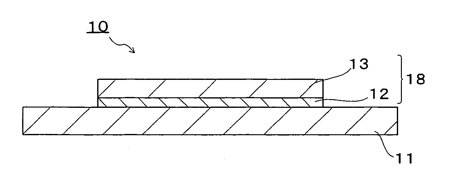
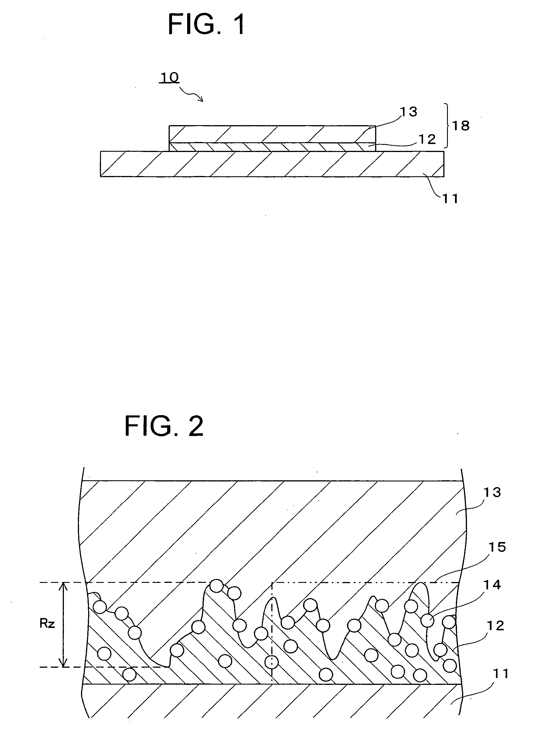
[0031]FIG. 1 schematically shows a section of a circuit board 10 of the first embodiment of the present invention. FIG. 2 schematically shows a section of an interface of a resin layer 12 and a conductive metal layer 13 under magnification.

[0032] As shown in FIGS. 1 and 2, the circuit board 10 is constructed by a substrate 11, the nonconductive resin layer 12 which is selectively formed on the substrate 11 and contains fine metal particles 14, and a conductive metal layer 13 which is formed in contact with the fine metal particles 14 exposed from the resin layer 12, on the resin layer 12. A conductor pattern 18 is formed by the resin layer 12 that is a base pattern, and the conductive metal layer 13 that is a plating deposition film.

[0033] In this case, the substrate 11 is composed of a nonconductive material, and is specifically composed of, for exam...

second embodiment

[0070] In a second embodiment, the case where a conductor pattern is formed by using a dry type developing device will be described.

[0071]FIG. 6 schematically shows a section of a circuit board 50 of the second embodiment of the present invention. FIG. 7 schematically shows a section of an interface of a resin layer 52 and a conductive metal layer 53 under magnification.

[0072] As shown in FIGS. 6 and 7, the circuit board 50 is constructed by a substrate 51, the nonconductive resin layer 52 which is selectively formed on the substrate 51 and contains fine metal particles 54, and a conductive metal layer 53 which is formed in contact with the fine metal particles 54 exposed from the resin layer 52, on the resin layer 52. In this case, a conductor pattern 58 is formed by the resin layer 52 that is a base pattern, and the conductive metal layer 53 that is a plating deposition film.

[0073] In this case, resins which form the substrate 51 and the resin layer 52, and a material which com...

third embodiment

[0099] In this case, a multilayer circuit board formed based on the manufacturing apparatus and the manufacturing method of the circuit board shown in the above described first or second embodiment, and its forming process will be described with reference to FIG. 11, and FIGS. 12A to 12G. In this case, one example using the manufacturing apparatus used for forming the circuit board 10 in the first embodiment will be shown.

[0100]FIG. 11 is a view schematically showing a section of a multilayer circuit board 400. FIGS. 12A to 12G are views schematically showing sections in the respective forming steps of the multilayer circuit board 400. In this case, the nonconductive layer containing the fine metal particles, which is called the resin layer in the first and second embodiment, will be called a metal containing resin layer. The nonconductive layer formed of only a resin is called an insulation layer.

[0101] As shown in FIG. 11, in the multilayer circuit board 400, a first conductor p...


PUM

PropertyMeasurementUnit
heightaaaaaaaaaa
lengthaaaaaaaaaa
lengthaaaaaaaaaa

Abstract

A circuit board includes a substrate, a nonconductive resin layer selectively formed on the substrate and containing fine metal particles, and a conductive metal layer formed on the resin layer, in contact with the fine metal particles which are exposed from the resin layer. A surface of the resin layer has irregularities, in an interface between the resin layer and the conductive metal layer. In a roughness curve of a section of the resin layer, in a case of an wavelength (λc) at the boundary of a roughness component and a waviness component is 1 μm, a maximum height (Rz) per reference length (1r) of 1 μm is 20 nm to 500 nm.

Description

CROSS-REFERENCE TO THE INVENTION [0001] This application is based upon and claims the benefit of priority from the prior Japanese Patent Application No. 2005-271211, filed on Sep. 16, 2005; the entire contents 6f which are incorporated herein by reference. BACKGROUND OF THE INVENTION [0002] 1. Field of the Invention [0003] The present invention relates to a circuit board having fine pitch wiring patterns suitable for being mounted and packaged on a semiconductor element, a chip component and the like, and a manufacturing method of the circuit board. [0004] 2. Description of the Related Art [0005] Conventionally, as a method for manufacturing a circuit board, a method using, for example, electrostatic transfer is adopted. In manufacture of circuit boards by using this method, an art of forming a conductor pattern by applying dry-type electrophotographic technology by using a toner to which a catalyst material active in an electroless plating bath is added is disclosed (see JP-A 58-57...

Claims


Application Information

Patent Timeline
Patent Type & Authority Applications(United States)
IPC IPC(8): G11B5/64
CPCH05K1/095H05K3/1266H05K3/182H05K3/246Y10T428/24355H05K2201/0347H05K2203/0517H05K2203/095H05K2201/0212G03G15/224G03G15/6585G03G15/6591
Inventor IIDA, ATSUKOISHII, KOICHISHINJIYO, YASUSHIYASUMOTO, TAKAAKIYANASE, NAOKO
Owner KK TOSHIBA
Why Eureka
Try Eureka