Manufacturing of optoelectronic devices

a manufacturing field and optoelectronic technology, applied in the field of manufacturing of optoelectronic devices, can solve the problems of reducing the yield of useful devices, adding extra processing steps, and scribing too deeply into one or more layers,

Inactive Publication Date: 2007-03-22
NANOSOLAR
View PDF6 Cites 101 Cited by
  • Summary
  • Abstract
  • Description
  • Claims
  • Application Information

AI Technical Summary

Problems solved by technology

This patterning adds extra processing steps and often introduces complications that can reduce the yield of useful devices.
For example, laser patterning or mechanical scribing may result in a condition known as overscribing where the scribing cuts too deeply into one or more layers.
Similarly, such scribing techniques may result in underscribing where the scribing does not cut sufficiently deep into one or more layers.
Furthermore, many scribing techniques can generate debris that may be inadvertently and undesirably incorporated into the finished devices.
All of these effects may interfere with proper device performance or cause catastrophic failure of devices and thereby add to the overall cost of useful devices.
Techniques for singulation into individual cells, e.g., laser scribing, often can not be used on such cells because of the associated risk of also cutting the underlying bottom electrode (e.g. Mo).

Method used


Image

  • Manufacturing of optoelectronic devices
  • Manufacturing of optoelectronic devices
  • Manufacturing of optoelectronic devices

Examples


Embodiment Construction

[0012] Although the following detailed description contains many specific details for the purposes of illustration, anyone of ordinary skill in the art will appreciate that many variations and alterations to the following details are within the scope of the invention. Accordingly, the exemplary embodiments of the invention described below are set forth without any loss of generality to, and without imposing limitations upon, the claimed invention.

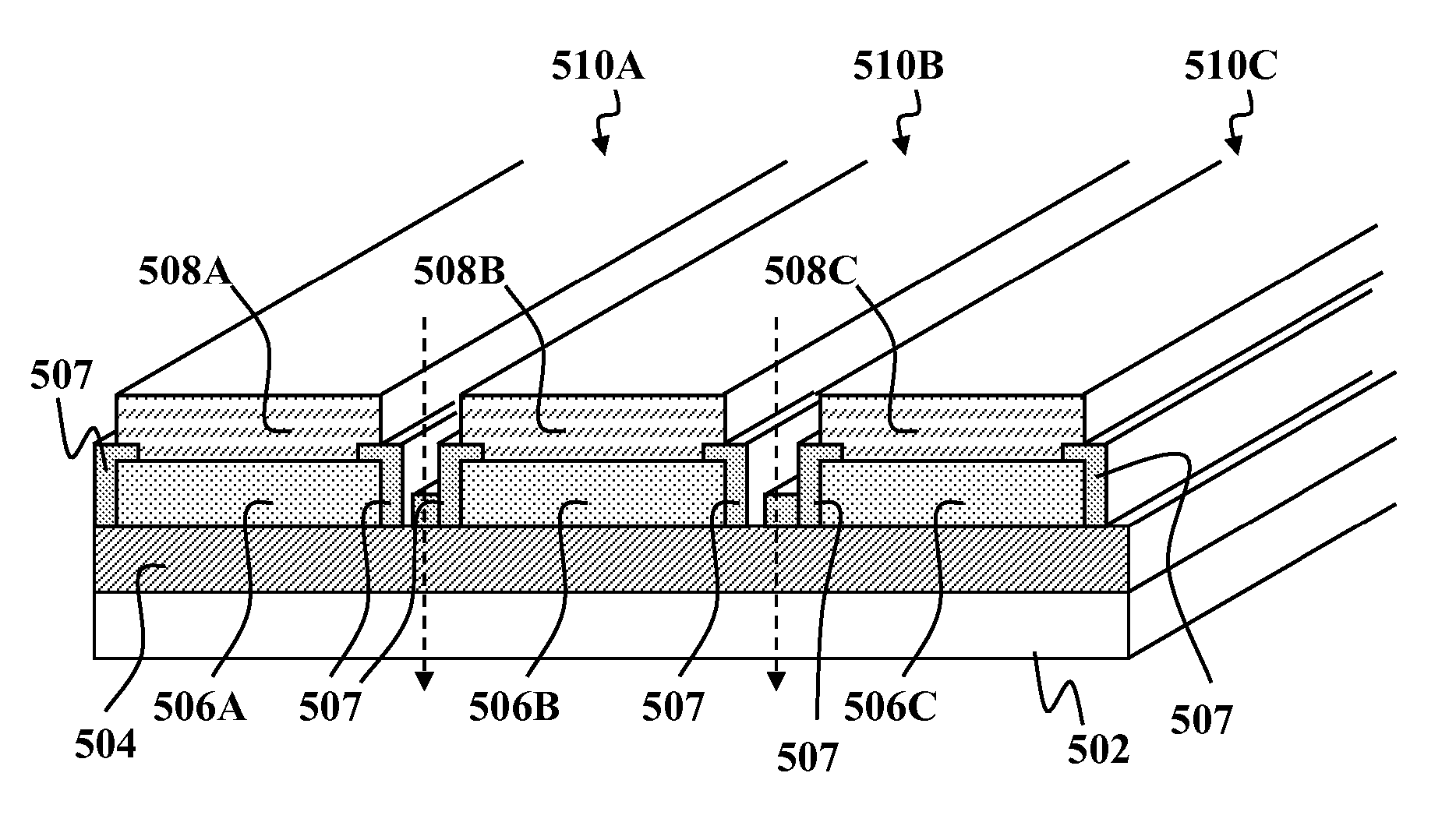
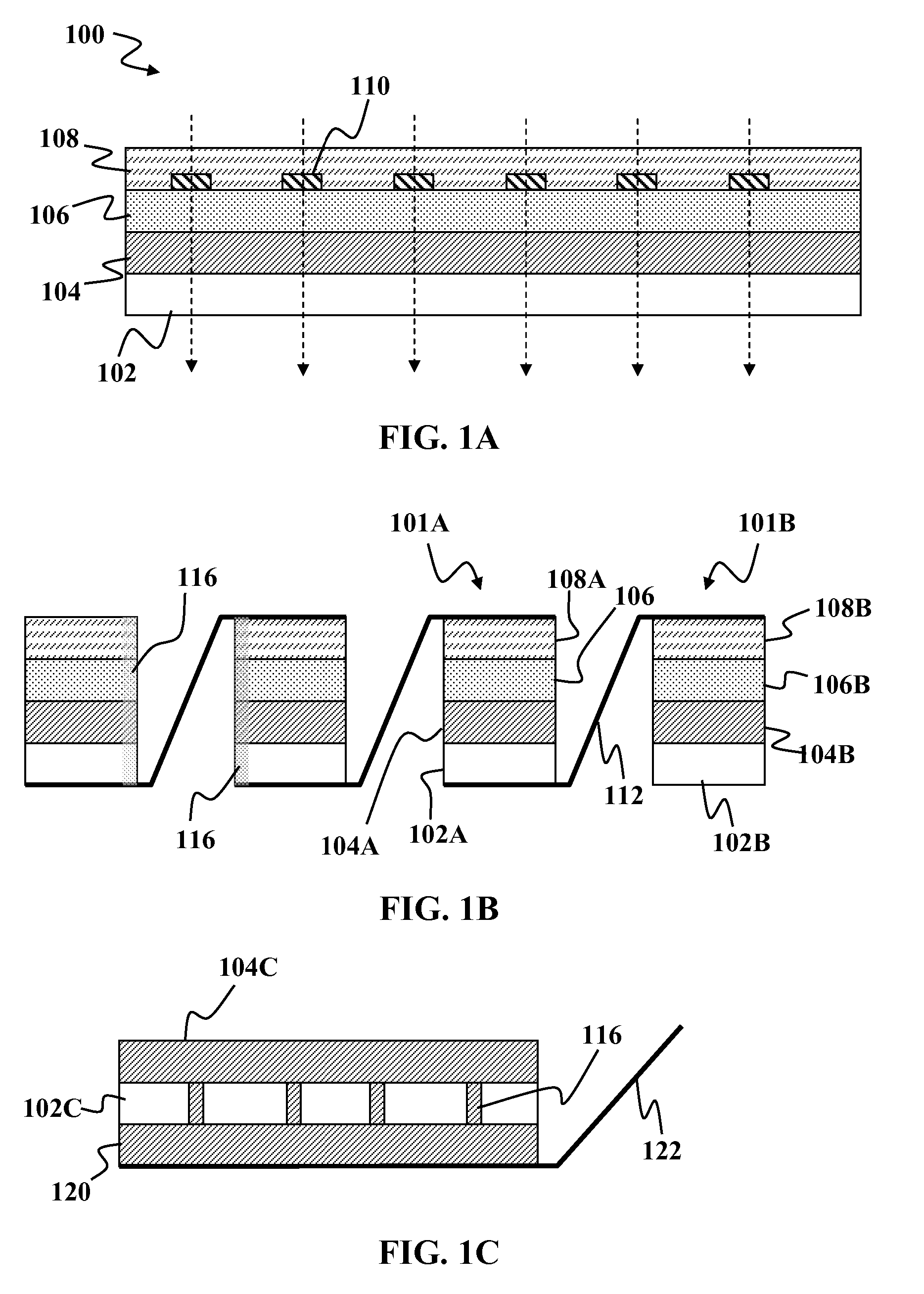
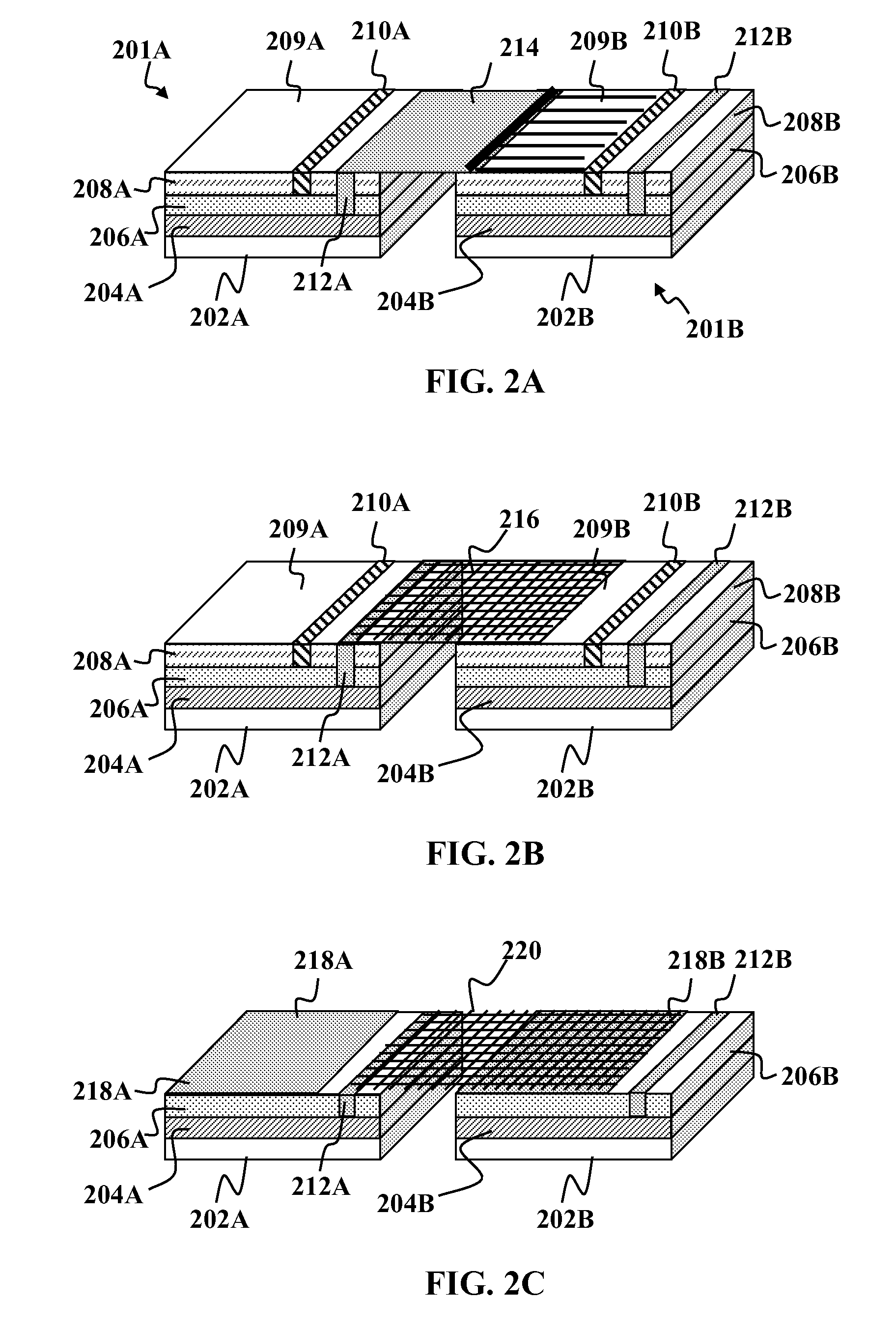
[0013] Optoelectronic devices may be manufactured less expensively and by cutting an unpatterned (or substantially unpatterned) layered structure into individual sections. According to embodiments of the present invention, an optoelectronic device may be manufactured in a roll-to-roll fashion with at least one but preferably more if not all of the individual layers that would normally be patterned being not patterned. Instead, a layered structure is formed, e.g., by one or more thin-film layer depositions. The layered structure is cut enti...


PUM


Abstract

A method for manufacturing optoelectronic devices is disclosed. A layered structure may be formed with a plurality of layers including a bottom electrode layer, a top electrode layer, and one or more active layers between the top and bottom electrode layers. The layered structure is divided into one or more separate device module sections by cutting through one or more of the layers of the layered structure. At least one of the layers is an unpatterned layer at the time of cutting. Each of the resulting device module sections generally includes a portion of the active layer disposed between portions of the top and bottom electrode layers. An edge of a device section may optionally be protected against undesired electrical contact between two or more of the bottom electrode, top electrode and active layer portions. Two or more device module sections may be assembled into a device and connected in series by electrically connecting the bottom electrode layer portion of one device section to the top electrode layer portion of another device module section.

Description

FIELD OF THE INVENTION [0001] This invention is related to manufacturing of optoelectronic devices and specifically to methods for roll-to-roll manufacturing of optoelectronic device modules on flexible foil substrates. BACKGROUND OF THE INVENTION [0002] Optoelectronic devices interact with radiation and electric current. The interaction can be photoelectric where the device converts incident radiant energy (e.g., in the form of photons) into electrical energy. Optoelectronic devices often tend to be high voltage and low current devices. Currently many optoelectronic devices, e.g., thin-film photovoltaic (PV) cells and organic light-emitting diodes (OLEDs) are made by depositing patterns of material on a substrate to form the various device layers, e.g., a bottom electrode, an active layer stack and a top electrode (plus auxiliary layers), of individual devices. For example, in the case of PV cells, typically all the bottom and top electrodes as well as the active PV layer stack are...

Claims


Application Information

Patent Timeline
Patent Type & Authority Applications(United States)
IPC IPC(8): H01L21/00
CPCH01L31/1876Y02E10/50H01L31/0475H01L31/0504H01L31/0508H01L31/02167H01L31/0445Y02P70/50
Inventor PICHLER, KARL
Owner NANOSOLAR
Why Eureka
Try Eureka