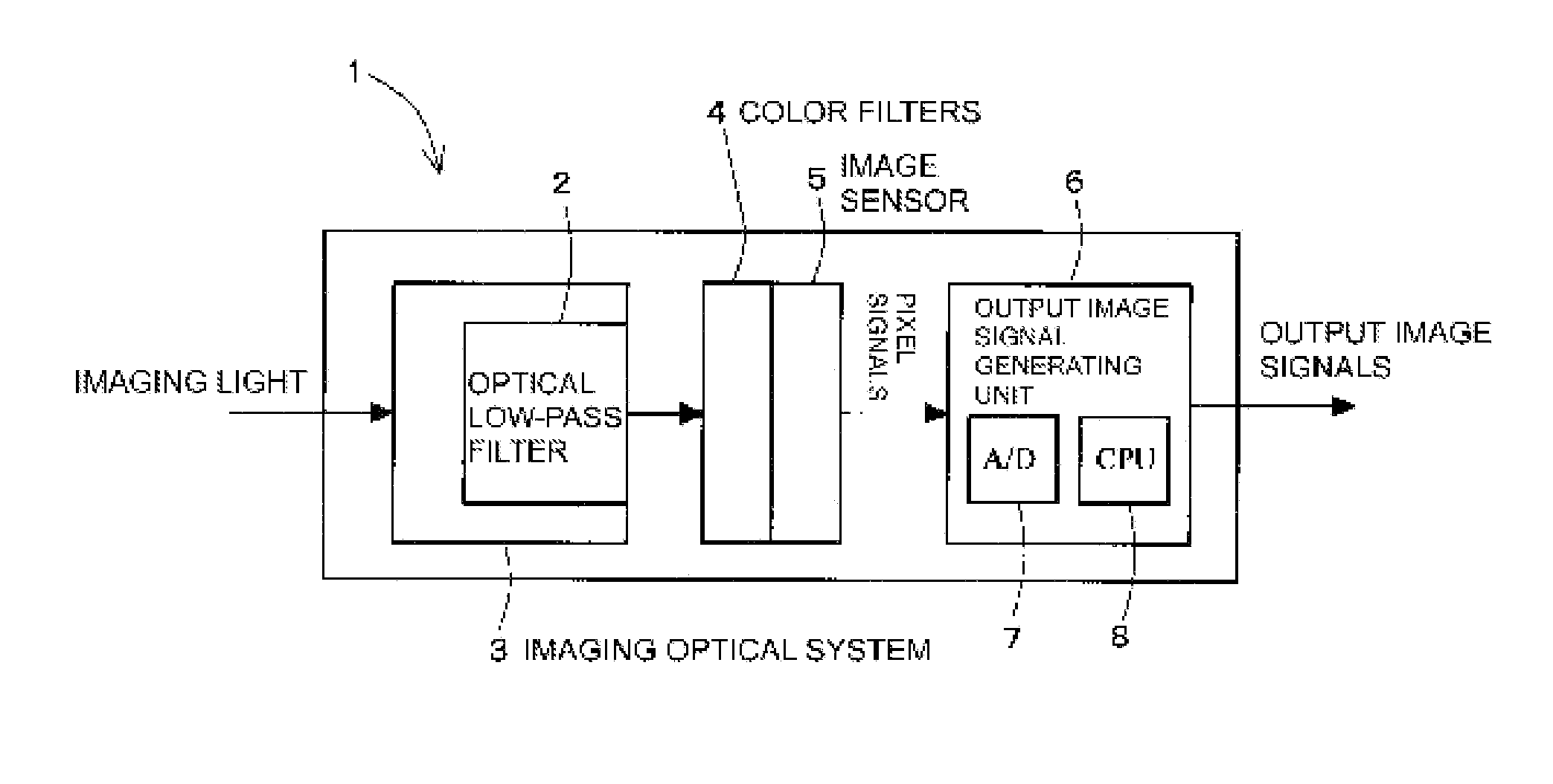
Imaging device

a low-pass filter and image processing technology, applied in the field of image processing devices, can solve the problems of false colors, the cutoff frequency fc of the optical low-pass filter cannot be set lower than half the sampling frequency (nyquist frequency), and the accuracy of the exact color reproduction. reproducibility and resolution ability can be improved

Active Publication Date: 2007-03-29
RDA TECH
View PDF14 Cites 8 Cited by
  • Summary
  • Abstract
  • Description
  • Claims
  • Application Information

AI Technical Summary

Benefits of technology

[0010] The occurrence of false colors for each color may be prevented by setting the cutoff frequency fc of the optical low-pass filter to a value lower than the Nyquist frequency for the sampling frequency in the longitudinal and lateral directions for R and B, which is the lowest sampling frequency among those of R, G, and B. However, this has a disadvantage of the lack of signals for the G component, so that the resolution of the generated output image is reduced and the image is blurred.
[0011] As shown in FIGS. 3 and 4, for an image sensor in which color filters are arranged in the Bayer pattern on imaging pixels arranged as a 45° oblique squared grid (pixel pitch: d), the cutoff frequency fc of the optical low-pass filter is preferably set lower than the Nyquist frequency for the sampling frequency of every color. In practice, to avoid sacrificing the resolution, the cutoff frequency fc is set to a value around fs / 2 (fs: sampling frequency of the image sensor) with respect to the sampling frequency in the oblique direction for G, because G has a high effect on vision. While this cutoff frequency fc can filter out unnecessary high frequencies in the oblique direction for G, it passes frequencies higher than the Nyquist frequencies in the other directions, i.e., the longitudinal and lateral directions, and in the longitudinal, lateral, and oblique directions for the other colors R and B. Therefore, as in the above-described squared grid arrangement, there is a disadvantage that pixel signals for these colors are not properly estimated and false colors tend to occur. Conversely, the occurrence of false colors may be prevented by setting the cutoff frequency fc with respect to the sampling frequency of the R and B components. However, this poses a problem that the resolution of the output image is reduced and the image is blurred.
[0013] The present invention has been made to solve these problems and aims to provide an imaging device capable of improving the color reproduction ability and the resolution ability to the level of a three-chip image sensor while using a simple single-chip image sensor.
[0020] According to the present invention, both the color reproduction ability and the resolution ability can be improved to the level of a three-chip image sensor while a simple single-chip image sensor is used.

Problems solved by technology

Thus, while a three-chip image sensor never causes false colors because each pixel receives signals of R, G, and B, a single-chip image sensor involves difficulty in reproducing exact colors and tends to cause false colors.
Further consideration of the mechanism causing the tendency of false colors poses a problem that, as shown in FIG. 2 or 4, the cutoff frequency fc of an optical low-pass filter has not been able to be set lower than half the sampling frequency (Nyquist frequency) of every color.
While this cutoff frequency fc can filter out unnecessary high frequencies in the longitudinal and lateral directions for G, it passes frequencies higher than the Nyquist frequency in the longitudinal and lateral directions for R and B and the Nyquist frequencies in the oblique direction for R, G, and B. Therefore, there is a disadvantage that pixel signals for these colors are not properly estimated and false colors tend to occur.
The occurrence of false colors for each color may be prevented by setting the cutoff frequency fc of the optical low-pass filter to a value lower than the Nyquist frequency for the sampling frequency in the longitudinal and lateral directions for R and B, which is the lowest sampling frequency among those of R, G, and B. However, this has a disadvantage of the lack of signals for the G component, so that the resolution of the generated output image is reduced and the image is blurred.

Method used


Image

  • Imaging device
  • Imaging device
  • Imaging device

Examples


example 1

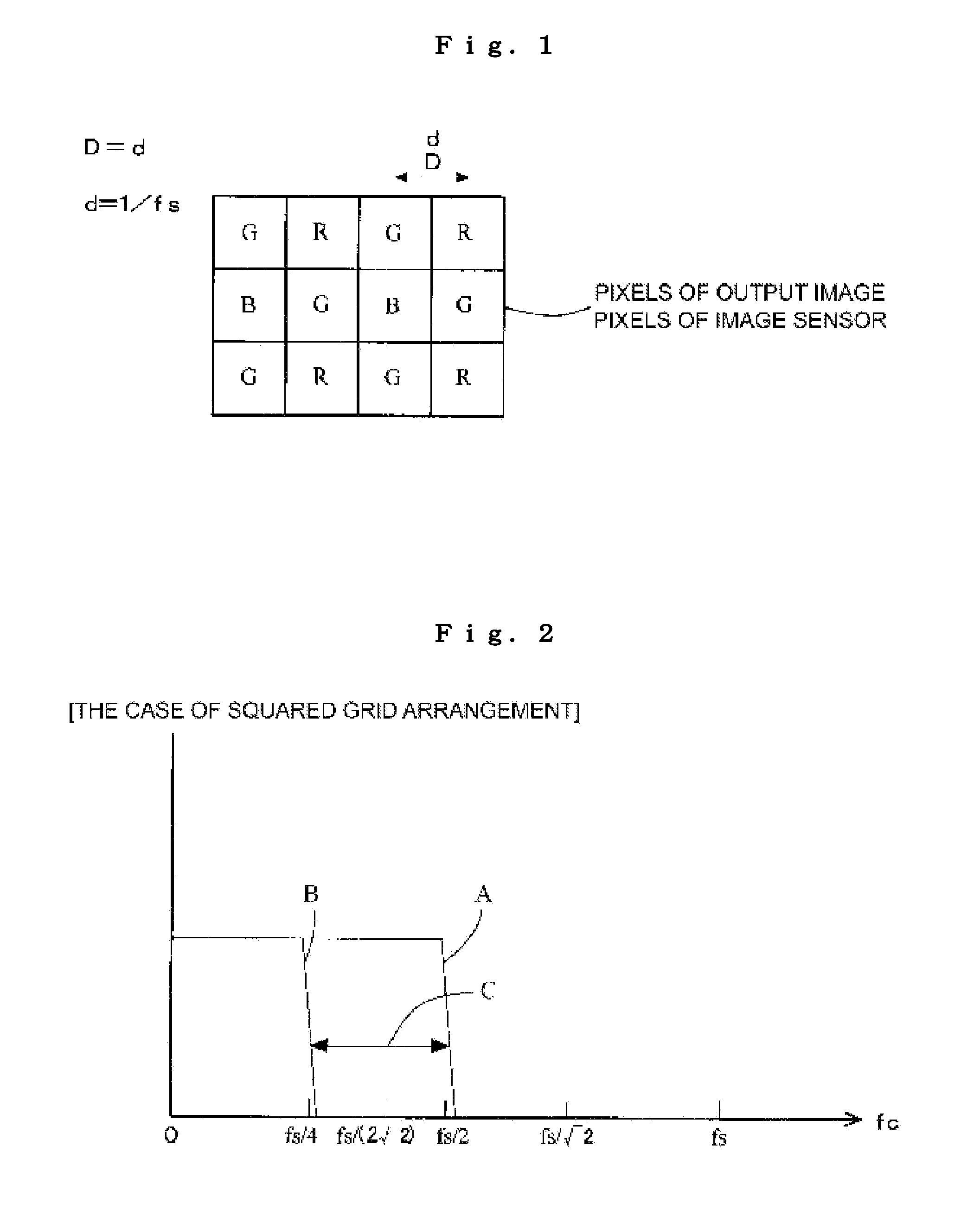
[0069] In the example 1, as shown in FIG. 14, the image sensor 5 was used in which pixels were arranged as a squared grid and the ratio k of the pixel pitch D of the output image to the pixel pitch d of the image sensor 5 was 1.5 (D=1.5d). As can be seen from FIG. 14, since 2.25 pixel signals were sampled for an output image signal for one pixel, N is 2.25.

example 2

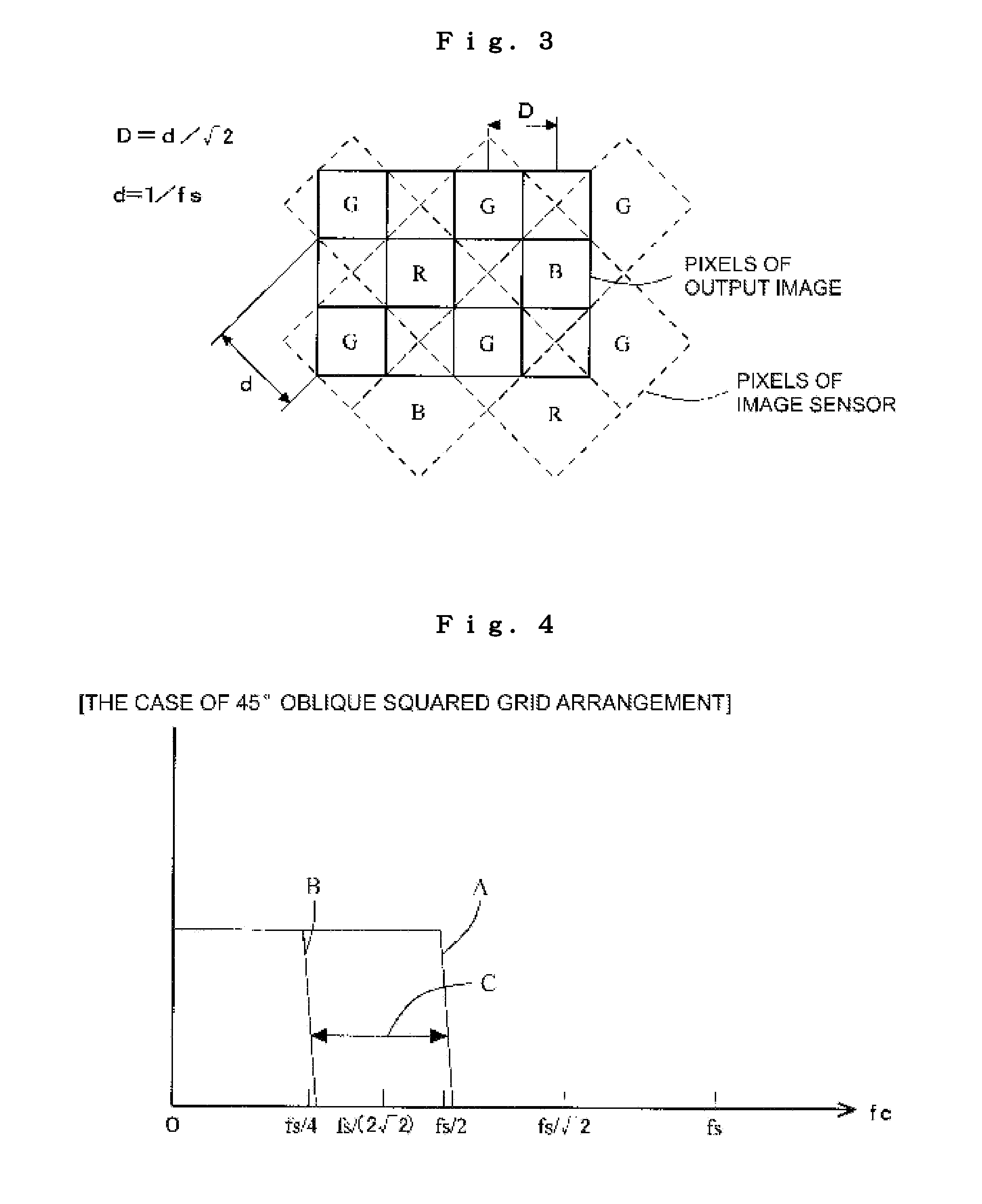
[0070] In the example 2, as shown in FIG. 15, the image sensor 5 was used in which pixels were arranged as a squared grid and the ratio k of the pixel pitch D of the output image to the pixel pitch d of the image sensor 5 was 2 (D=2d). As can be seen from FIG. 15, since 4 pixel signals were sampled for an output image signal for one pixel, N is 4.

example 3

[0071] In the example 3, as shown in FIG. 16, the image sensor 5 was used in which pixels were arranged as a squared grid and the ratio k of the pixel pitch D of the output image to the pixel pitch d of the image sensor 5 was 4 (D=4d). As can be seen from FIG. 16, since 16 pixel signals were sampled for an output image signal for one pixel, N is 16.


PUM


Abstract

Frequency characteristics of an optical low-pass filter (2) are set in such a way that a first false color passing rate indicative of the rate of frequency components passing through a frequency component region not lower than the Nyquist frequency fa for the lowest sampling frequency fs among the sampling frequencies in the longitudinal, the lateral, and the oblique directions for each color in an image sensor (5), i.e. a frequency component region lower than one half of the Nyquist frequency fs of the sampling frequency fs of the image sensor (5), is not higher than a specified value. An output image signal is created from a pixel signal created by the image sensor (5) so that N pixel signals (N is real number of 2 or above) created by the image sensor (5) correspond to one output image signal.

Description

CROSS-REFERENCE TO RELATED APPLICATION [0001] This application is a continuation under 35 USC 120 of co-pending International application PCT / JP2005 / 007187 filed on Apr. 7, 2005. International application PCT / JP2005 / 007187 claims priority to Japanese application 2004-156083 filed on May 26, 2004. The entire contents of each of these applications are incorporated herein by reference.TECHNICAL FIELD [0002] The present invention relates to an imaging device for apparatus such as digital cameras and digital video cameras, and more particularly to an imaging device that takes an image of an object with a single-chip image sensor. BACKGROUND ART [0003] Conventionally, when an imaging device for taking color images is configured with a single-chip image sensor, photodiodes (pixels) are arranged like a squared grid or a 45° oblique squared grid, and color filters corresponding to color components such as R (red), G (green), and B (blue) are arranged on the photoreceptive surface of the resp...

Claims


Application Information

Patent Timeline
Patent Type & Authority Applications(United States)
IPC IPC(8): H04N9/04H04N9/07H04N9/093
CPCH04N9/093H04N9/045H04N23/84H04N23/15H04N25/134H04N23/10H04N23/12
Inventor SEI, MASAFUMIMASUDA, TAKASHI
Owner RDA TECH
Why Eureka
Try Eureka