Electroless copper plating solution and electroless copper plating method

a technology of electroless copper plating and electroless copper, which is applied in the direction of application, liquid/solution decomposition chemical coating, inks, etc., can solve the problems of low plating reactivity, low adhesive strength, and difficult to plate uniformly over the entire substra

Inactive Publication Date: 2007-03-29
JX NIPPON MINING & METALS CO LTD
View PDF6 Cites 17 Cited by
  • Summary
  • Abstract
  • Description
  • Claims
  • Application Information

AI Technical Summary

Benefits of technology

[0007] As a result of diligent study, the inventors discovered that when a first reducing agent (such as formalin or glyoxylic acid) and hypophosphorous acid or a hypophosphite (such as sodium hypophosphite, potassium hypophosphite, or ammonium hypophosphite) are used at the same time in an electroless copper plating solution, the initial plating reactivity via a metal catalyst is higher, and that when a stabilizer to inhibit copper deposition (such as 2,2′-bipyridyl, imidazole, nicotinic acid, thiourea, 2-mercaptobenzothiazole, sodium cyanide, or thioglycolic acid) is also used at the same time, excessive deposition reactions generated in some portion will be prevented, and as a result, uniform plating can be achieved at lower temperatures even on a semiconductor wafer (such as a silicon wafer, a semiconductor wafer made of GaAs·InP or the like, or these wafers with a tantalum nitride film, titanium nitride film, tungsten nitride film, tantalum film or the like formed thereon) or other such mirror surface with an average surface roughness of less than 10 nm. The present invention is particularly effective in the production of thin films with a thickness of 500 nm or less.

Problems solved by technology

Conventionally, when a semiconductor wafer or other such mirror surface was electroless plated with copper, the plating reactivity was low and it was difficult to plate uniformly over the entire substrate.
Examples of problems currently encountered in electroless copper plating include low adhesive strength and poor plating uniformity when a copper film is formed over a barrier metal layer such as tantalum nitride.
This electroless copper plating solution is stable and has a high copper deposition speed, but it is difficult to plate uniformly when this solution was used on a semiconductor wafer or other such mirror surface.

Method used


Image

  • Electroless copper plating solution and electroless copper plating method
  • Electroless copper plating solution and electroless copper plating method

Examples


example 1

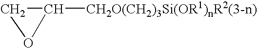
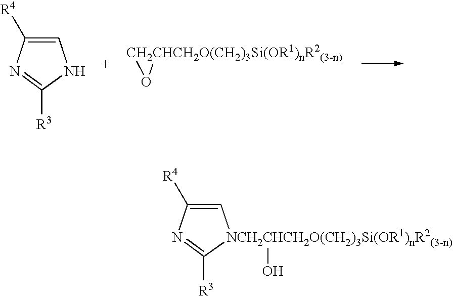
[0039] The above-mentioned silicon wafer with the tantalum nitride film was immersed for 5 minutes at 50° C. in a pretreatment agent for plating prepared by adding a palladium chloride aqueous solution so as to be 50 mg / L to 0.16 wt % aqueous solution of the silane coupling agent that was the equimolar reaction product of imidazole and γ-glycidoxypropyltrimethoxysilane. After this, the wafer was heat treated for 15 minutes at 200° C., and then was electroless plated with copper for 5 minutes at 60° C. The composition of the plating solution was copper sulfate 0.04 mol / L, ethylenediaminetetraacetate 0.4 mol / L, formalin 0.1 mol / L, sodium hypophosphite 0.1 mol / L, and 2,2′-bipyridyl 10 mg / L, and the pH was 12.5 (pH regulator: sodium hydroxide). The plating film was formed uniformly without unevenness over the entire surface, and the film thickness was 50 nm.

example 2

[0040] The above-mentioned silicon wafer with the tantalum nitride film was pretreated by the same method as in Example 1, after which the wafer was electroless plated with copper for 5 minutes at 60° C. The composition of the plating solution was copper sulfate 0.04 mol / L, ethylenediaminetetraacetate 0.4 mol / L, glyoxylic acid 0.1 mol / L, hypophosphorous acid 0.1 mol / L, and 2,2′-bipyridyl 10 mg / L, and the pH was 12.5 (pH regulator: potassium hydroxide). The plating film was formed uniformly without unevenness over the entire surface, and the film thickness was 50 nm.

example 3

[0041] The above-mentioned silicon wafer with the tantalum nitride film was pretreated by the same method as in Example 1, after which the wafer was electroless plated with copper for 5 minutes at 60° C. The composition of the plating solution was copper sulfate 0.04 mol / L, ethylenediaminetetraacetate 0.4 mol / L, formalin 0.1 mol / L, ammonium hypophosphite 0.1 mol / L, and 2,2′-bipyridyl 10 mg / L, and the pH was 12.5 (pH regulator: sodium hydroxide). The plating film was formed uniformly without unevenness over the entire surface, and the film thickness was 50 nm.


PUM

PropertyMeasurementUnit
thicknessaaaaaaaaaa
surface roughnessaaaaaaaaaa
concentrationaaaaaaaaaa

Abstract

An object is to provide an electroless copper plating solution that realizes uniform plating at lower temperatures, when the electroless copper plating is performed on a semiconductor wafer or other such mirror surface on which a plating reaction hardly occurs. An electroless copper plating solution, wherein, along with a first reducing agent, hypophosphorous acid or a hypophosphite is used as a second reducing agent, and a stabilizer to inhibit copper deposition is further used at the same time. Examples of the first reducing agent include formalin and glyoxylic acid, while examples of the hypophosphite include sodium hypophosphite, potassium hypophosphite, and ammonium hypophosphite. Examples of the stabilizer to inhibit copper deposition include 2,2′-bipyridyl, imidazole, nicotinic acid, thiourea, 2-mercaptobenzothiazole, sodium cyanide, and thioglycolic acid.

Description

TECHNICAL FIELD [0001] This invention relates to an electroless copper plating solution used primarily in the electroless copper plating of a mirror surface such as a semiconductor wafer, and to an electroless copper plating method that makes use of this plating solution. BACKGROUND ART [0002] Electroless copper plating holds great promise as a method to form a copper film for ULSI fine wiring, and as a replacement for the sputtering and electrolytic copper plating methods currently in use. [0003] Conventionally, when a semiconductor wafer or other such mirror surface was electroless plated with copper, the plating reactivity was low and it was difficult to plate uniformly over the entire substrate. Examples of problems currently encountered in electroless copper plating include low adhesive strength and poor plating uniformity when a copper film is formed over a barrier metal layer such as tantalum nitride. [0004] Formalin is typically used as a reducing agent for an electroless co...

Claims


Application Information

Patent Timeline
Patent Type & Authority Applications(United States)
IPC IPC(8): B05D1/18C23C18/40C23C18/31H01L21/288
CPCH01L21/288C23C18/405C23C18/1683C23C18/1851
Inventor YABE, ATSUSHISEKIGUCHI, JUNNOSUKEIMORI, TORUFUJIHIRA, YOSHIHISA
Owner JX NIPPON MINING & METALS CO LTD
Why Eureka
Try Eureka