Semiconductor device

a semiconductor and device technology, applied in the direction of semiconductor devices, basic electric elements, electrical appliances, etc., can solve the problems of increased power dissipation, deterioration of performance, and large inconvenience, and achieve satisfactory mechanical strength of semiconductor substrates, performance and breakdown voltage.

Inactive Publication Date: 2007-04-05
MITSUBISHI ELECTRIC CORP
View PDF6 Cites 12 Cited by
  • Summary
  • Abstract
  • Description
  • Claims
  • Application Information

AI Technical Summary

Benefits of technology

[0009] An object of the invention is to provide a semiconductor device in which a main current flows in the thickness direction of the semiconductor substrate and which offers satisfactory performance and breakdown voltage and also satisfactory mechanical strength of the semiconductor substrate, and which needs no inconvenient control of the exposure system etc. during photolithography process.
[0011] According to the first aspect of the semiconductor device of the invention, the first thickness, for example, can be set so that the semiconductor wafer is less likely to crack or break during manufacturing and so that no special focal depth control is needed for the exposure system etc.; this reduces occurrence of defects during manufacturing and reduces the manufacturing cost, and offers a semiconductor device achieving a balance between the reduction of on-state resistance and the sustainment of breakdown voltage.
[0013] According to the second aspect of the semiconductor device of the invention, the first thickness, for example, can be set so that the semiconductor wafer is less likely to crack or break during manufacturing and so that no special focal depth control is needed for the exposure system etc.; this reduces occurrence of defects during manufacturing and reduces the manufacturing cost, and offers a semiconductor device achieving a balance between reducing the on-state resistance and keeping the breakdown voltage. Furthermore, filling the at least one recess with a conductor layer enhances the mechanical strength of the semiconductor substrate and facilitates handling of the semiconductor substrate during semiconductor device manufacturing process.

Problems solved by technology

On the other hand, increasing the semiconductor substrate thickness increases the on-state resistance, which increases power dissipation and deteriorates performance.
There is an optimum substrate thickness also from the viewpoint of photolithography process, since, if the semiconductor substrate is extremely thin, then existing exposure systems etc. need focal depth control during formation of a given pattern by photolithography on the semiconductor substrate, causing great inconvenience.
Use of epitaxial-growth substrates is proposed in order to satisfy these conditions, but thickening epitaxial-growth layers takes time and increases cost.

Method used


Image

  • Semiconductor device
  • Semiconductor device
  • Semiconductor device

Examples


first modification

L. First Modification

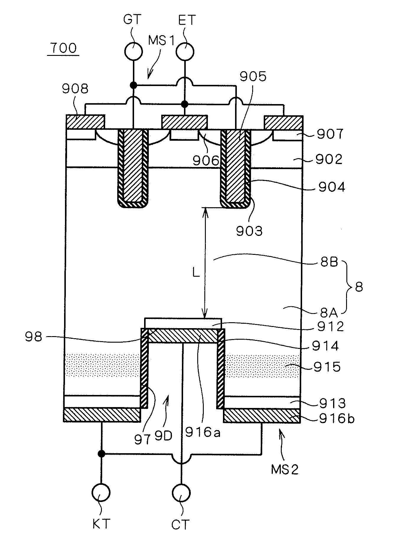
[0200] The semiconductor devices 700 and 700A of the seventh preferred embodiment have shown structures in which the N-type semiconductor regions 913 are provided in the surface of the mesa region 8A on the second main surface MS2 side; however, as shown in FIG. 36 as a semiconductor device 700B, P-type semiconductor regions 912a may replace the N-type semiconductor regions 913.

[0201] This structure does not need electrical separation between the P-type collector region 912 and the P-type semiconductor regions 912a, which removes the need for sidewall insulating films on the side surfaces of the recess 9D.

[0202] The semiconductor device 700B has a recess 9D filled with a conductor layer 920 with a common main electrode 916 lying over the surfaces of both of the P-type semiconductor regions 912a and the conductor layer 920. The common main electrode 916 is connected to the external terminal CT.

[0203] With this structure, when a same positive potential is appli...

second modification

M. Second Modification

[0206] In the semiconductor devices 700 and 700A of the seventh preferred embodiment, N-type semiconductor regions 913 are provided in the surface of the mesa region 8A on the second main surface MS2 side; however, as shown in FIG. 37 as a semiconductor device 700C, P-type semiconductor regions 912a may replace the N-type semiconductor regions 913, with P-type semiconductor regions 912b formed in the surface of the N-type semiconductor substrate 8 in the portions defining the sides of the recess 9D, where the P-type collector region 912 and the P-type semiconductor regions 912a are thus electrically connected through the P-type semiconductor regions 912b.

[0207] Also in the semiconductor device 700C, the recess 9D is filled with a conductive layer 920 and a common main electrode 916 is disposed over the surfaces of the P-type semiconductor regions 912a and the conductor layer 920. The common main electrode 916 is connected to the external terminal CT.

[0208] Wi...


PUM


Abstract

The present invention relates to a semiconductor device; in particular, an object of the invention is to provide a semiconductor device in which a main current flows in a direction of thickness of the semiconductor substrate and which offers satisfactory performance and breakdown voltage and also satisfactory mechanical strength of the semiconductor substrate, and which needs no inconvenient control of the exposure system etc. during photolithography process. In order to achieve the object, a semiconductor device has a semiconductor substrate (1) having a first main surface (MS1), a second main surface (MS2) opposite to the first main surface, and a recess (9) defined in the second main surface (MS2) by side surfaces (91) and a bottom surface (92), a semiconductor region (IP5) provided in the bottom surface (92) of the recess (9) of the semiconductor substrate (1), semiconductor regions (IP4) provided in the surface of a peripheral region 1A on the second main surface (MS2) side, and insulating films (IL) provided on the side surfaces (91) of the recess (9) to electrically insulate the semiconductor regions (IP4) and (IP5).

Description

TECHNICAL FIELD [0001] This application is a continuation of and is based upon and claims the benefit of priority under 35 U.S.C. §120 from U.S. Ser. No. 10 / 505,179, filed on Aug. 31, 2004, the entire contents of which are incorporated herein by reference.BACKGROUND ART [0002] In general, in a semiconductor device in which the main current flows in the direction of the thickness of the semiconductor substrate, the breakdown voltage increases as the semiconductor substrate thickness increases to a certain thickness determined by the resistivity of the substrate; the breakdown voltage becomes substantially fixed at the certain thickness or more. On the other hand, increasing the semiconductor substrate thickness increases the on-state resistance, which increases power dissipation and deteriorates performance. [0003] Thus, with a semiconductor device in which the main current flows in the thickness direction of the semiconductor substrate, the optimum substrate thickness is determined ...

Claims


Application Information

Patent Timeline
Patent Type & Authority Applications(United States)
IPC IPC(8): H01L29/74H01L21/08H01L21/331H01L29/06H01L29/08H01L29/32H01L29/739
CPCH01L29/0657H01L29/0834H01L29/32H01L2924/10158H01L29/66348H01L29/7397H01L29/872H01L29/47H01L2924/10155H01L21/02
Inventor TOKUDA, NORIFUMIKUSUNOKI, SHIGERU
Owner MITSUBISHI ELECTRIC CORP
Why Eureka
Try Eureka