Image sensor and method of fabricating the same

a technology of image sensor and manufacturing method, which is applied in the field of image sensor, can solve problems such as deteriorating the reproduction characteristics of image sensor, and achieve the effects of improving image reproduction characteristics, reducing white spots and/or dark currents

Active Publication Date: 2007-04-05
SAMSUNG ELECTRONICS CO LTD
View PDF7 Cites 35 Cited by
  • Summary
  • Abstract
  • Description
  • Claims
  • Application Information

AI Technical Summary

Benefits of technology

[0008] Example embodiments may provide an image sensor, and fabrication method thereof, capable of having

Problems solved by technology

However, on the surface of a semiconductor substrate constituting the image sensor, dangling bonds and the like may be produced if the surface is damaged during an ion implantation and/or etching process.
If t

Method used


Image

  • Image sensor and method of fabricating the same
  • Image sensor and method of fabricating the same
  • Image sensor and method of fabricating the same

Examples


Embodiment Construction

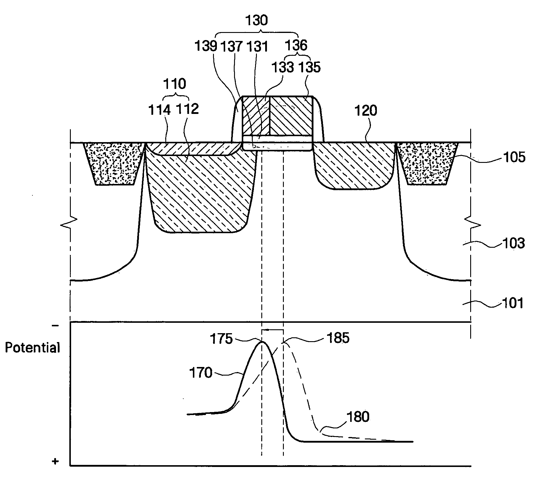
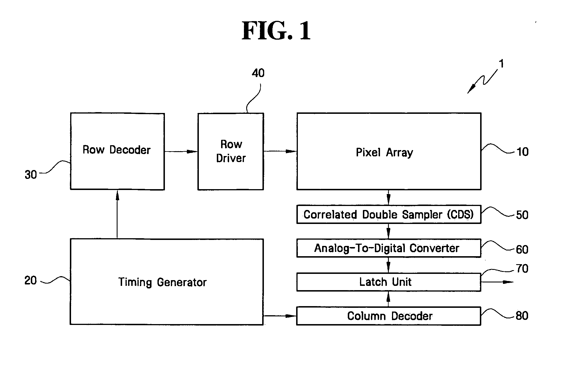
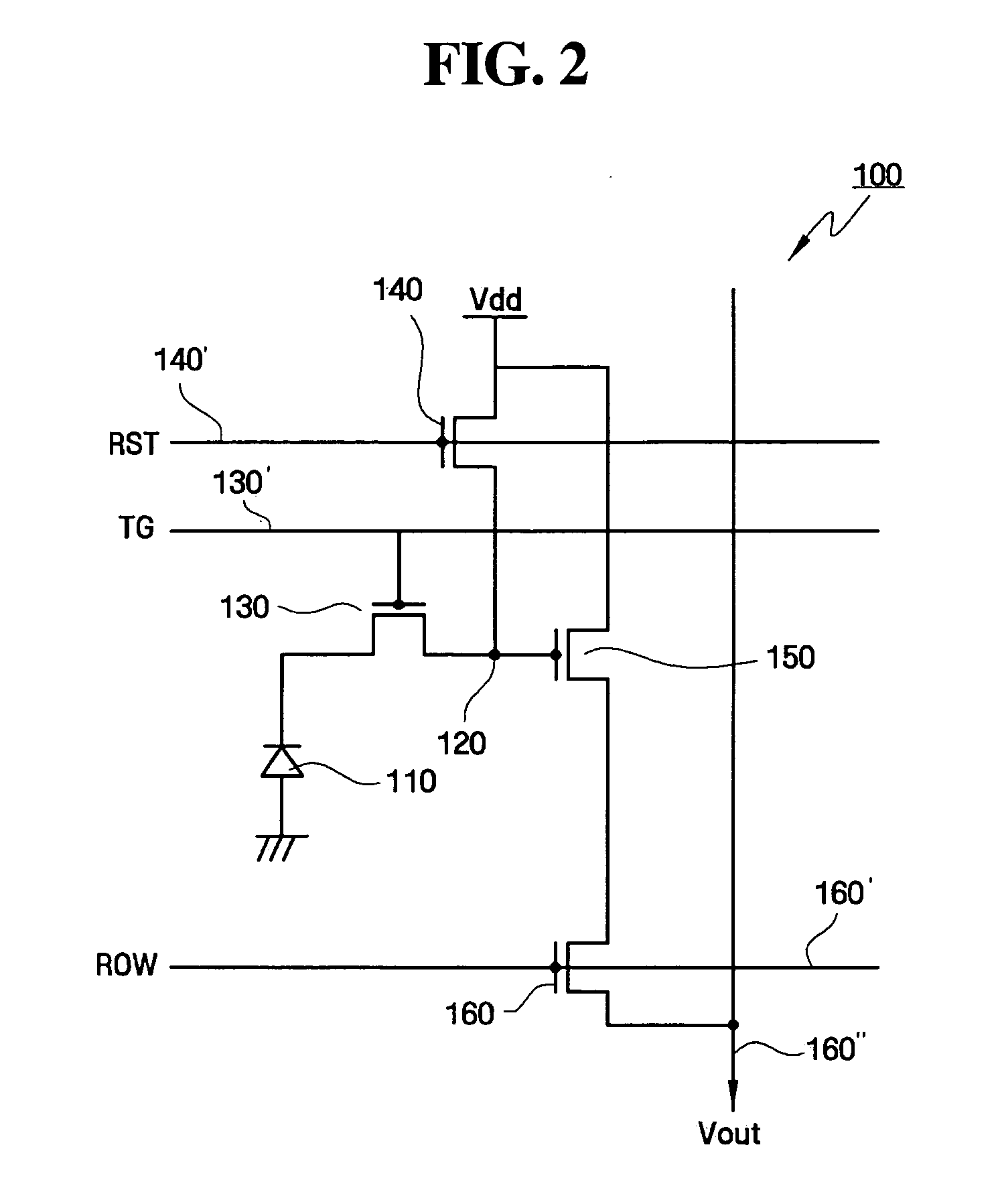
[0034] Various example, non-limiting embodiments will now be described more fully with reference the accompanying drawings. However, specific structural and functional details disclosed herein are merely representative for purposes of describing example, non-limiting embodiments. Example embodiments may, however, may be in many alternate forms and should not be construed as limited to only the example, non-limiting embodiments set forth herein.

[0035] Accordingly, example, non-limiting embodiments are provided so that this disclosure will be thorough and complete, and will fully convey the scope of the present invention to those skilled in the art, and the scope will be defined by the appended claims. Well-known device structures and technologies will not be described in detail in some example embodiments to avoid obscuring the example embodiments. Further, terms like “first conductivity type” and “second conductivity type” indicate conductive types opposite to each other, for examp...


PUM


Abstract

Example embodiments relate to an image sensor and a fabrication method thereof. An image sensor may include a semiconductor substrate. A charge transfer structure may be formed on the semiconductor substrate. The charge transfer structure may include a gate insulating film that may be formed on a channel region in the semiconductor substrate between a photoelectric conversion region and charge detection region, and a transfer gate electrode that may be formed on the gate insulating film that may have a region doped with a first conductivity type impurity-doped region and a second conductivity type impurity-doped region which may be adjacent to each other.

Description

PRIORITY STATEMENT [0001] This U.S. non-provisional application is based on and claims priority under 35 U.S.C. §119 from Korean Patent Application No. 10-2005-0093106, filed on Oct. 4, 2005 in the Korean Intellectual Property Office (KIPO), the entire contents of which is incorporated herein by reference. BACKGROUND [0002] 1. Field [0003] Example, non-limiting embodiments relate to an image sensor, for example, to an image sensor having improved image reproduction characteristics. [0004] 2. Description of the Related Art [0005] An image sensor is a device that may convert optical images to electrical signals. With the development of the computer and the communication industries, there may be an increasing demand for an image sensor having improved performance, for example, for use in digital cameras, camcorders, PCS's (Personal Communication Systems), gaming machines, security cameras, micro-cameras for medical applications, and / or robots. [0006] The unit pixel of the image sensor ...

Claims


Application Information

Patent Timeline
IPC IPC(8): H01L29/768
CPCH01L27/14603H01L27/14689H01L27/146
Inventor JUNG, SANG-ILYI, DUK-MIN
Owner SAMSUNG ELECTRONICS CO LTD
Why Eureka
Try Eureka