Circuit device including vertical transistors connected to buried bitlines and method of manufacturing the same

a technology of vertical transistors and transistors, which is applied in the direction of transistors, semiconductor devices, electrical equipment, etc., can solve the problems of short channel effect phenomenon generation and/or degrade the current driving performance of an active device such as a transistor, and achieve the effect of configuring the peripheral circui

Active Publication Date: 2007-04-05
SAMSUNG ELECTRONICS CO LTD
View PDF9 Cites 125 Cited by
  • Summary
  • Abstract
  • Description
  • Claims
  • Application Information

AI Technical Summary

Benefits of technology

[0011] Embodiments of the present invention provide a circuit device including vertical transistors and interconnection lines connecting the vertical transistors and methods of manufacturing the circuit device, which can reduce a substrate area required for a peripheral circuit region.
[0044] In another aspect, the present invention is directed to a method of manufacturing a circuit device including vertical transistors, the method comprising: providing a semiconductor substrate including a peripheral circuit region and left and right cell regions at both sides of the peripheral circuit region; forming bottom active regions on the semiconductor substrate to be spaced apart from one another in a column direction and to extend from the peripheral circuit region alternately to the left cell region and the right cell region in a row direction; forming channel pillars protruding from the bottom active regions in a vertical direction and arranged to be aligned in the row direction and spaced apart from one another; forming gate electrodes surrounding side walls of the channel pillars; forming buried bitlines extending along the bottom active regions, the bottom active regions including a bottom source / drain region; forming an upper source / drain region on the channel pillars; forming a first gate dielectric layer between the gate electrodes and the upper source / drain region; forming a second gate dielectric layer between the gate electrodes and the channel pillars; forming local interconnection lines contacting side surfaces of the gate electrodes in the peripheral circuit region and extending between the gate electrodes to commonly interconnect the gate electrodes in the peripheral circuit region, thereby configuring a peripheral circuit; forming signal lines electrically connected to upper surfaces of the channel pillars or to at least one of the local interconnection lines; and forming interconnection contacts electrically connecting the local interconnection line to the buried bitline of a different row from that of the commonly-connected gate electrodes or electrically connecting the local interconnection lines to the signal lines, thereby configuring the peripheral circuit.

Problems solved by technology

The reduction of the design rule commonly results in the generation of the short channel effect phenomenon and / or degraded current driving performance of an active device such as a transistor.

Method used


Image

  • Circuit device including vertical transistors connected to buried bitlines and method of manufacturing the same
  • Circuit device including vertical transistors connected to buried bitlines and method of manufacturing the same
  • Circuit device including vertical transistors connected to buried bitlines and method of manufacturing the same

Examples


Embodiment Construction

[0053] The present invention will now be described more fully with reference to the accompanying drawings, in which exemplary embodiments of the invention are shown. The invention may, however, be embodied in many different forms and should not be construed as being limited to the embodiments set forth herein; rather, these embodiments are provided so that this disclosure will be thorough and complete.

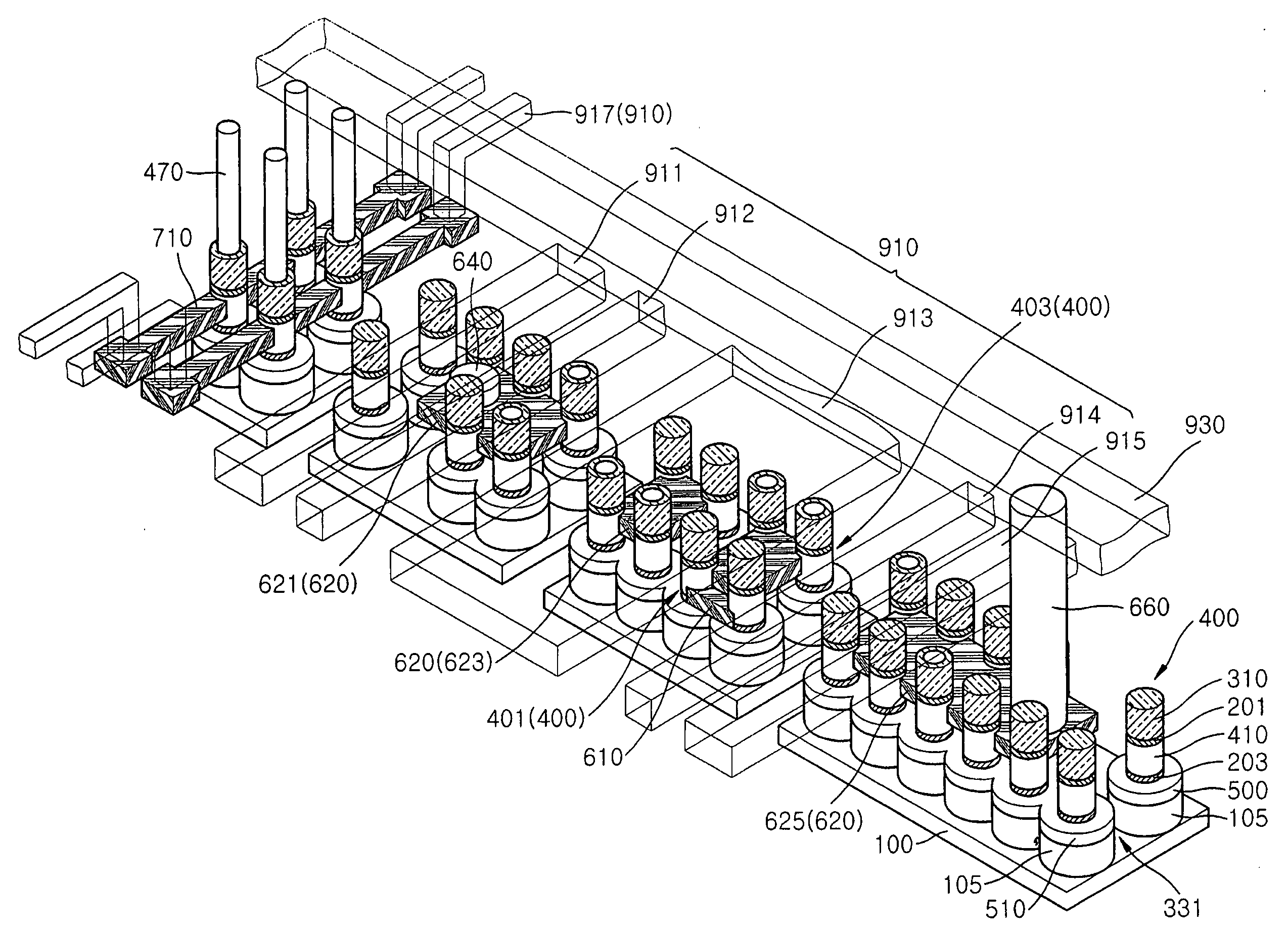
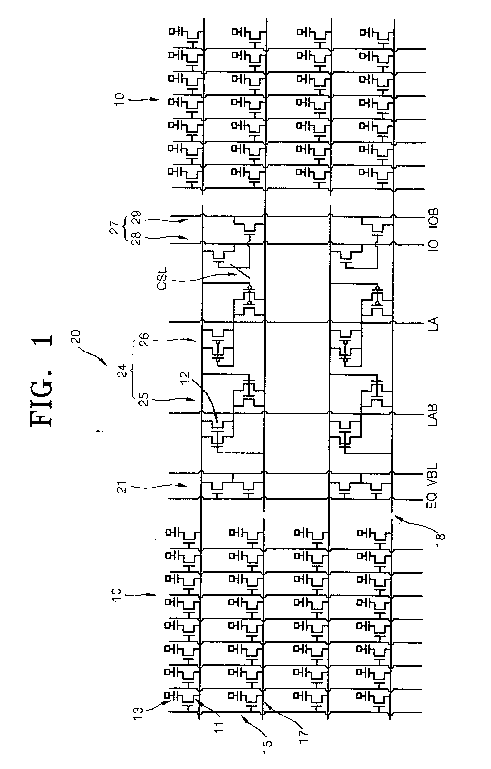
[0054] The present disclosure proposes vertical transistor structures and a technique for implementing a peripheral circuit device that includes an interconnection line structure for interconnecting the vertical transistor structures for construction of, for example, a sense amplifier, and methods for manufacturing the same.

[0055] The vertical transistor structures according to the embodiments of the present invention includes a channel pillar that preferably projects or extends in a vertical direction relative to a horizontal upper surface of the substrate, and serves as a channel r...


PUM


Abstract

In a circuit device including vertical transistors connected to buried bitlines and a method of manufacturing the circuit device, the circuit device includes a semiconductor substrate including a peripheral circuit region and left and right cell regions at both sides of the peripheral circuit region; bottom active regions arranged on the semiconductor substrate to be spaced apart from one another in a column direction and to extend from the peripheral circuit region alternately to the left cell region and the right cell region in a row direction; channel pillars protruding from the bottom active regions in a vertical direction and arranged to be aligned in the row direction and spaced apart from one another; gate electrodes provided with a gate dielectric layer and attached to surround side surfaces of the channel pillars; buried bitlines extending along the bottom active regions, the bottom active regions including a bottom source / drain region; local interconnection lines contacting side surfaces of the gate electrodes in the peripheral circuit region and extending between the gate electrodes to commonly interconnect the gate electrodes in the peripheral circuit region, thereby configuring a peripheral circuit; signal lines electrically connected to upper surfaces of the channel pillars or to at least one of the local interconnection lines; and interconnection contacts electrically connecting the local interconnection line to the buried bitline of a different row from that of the commonly-connected gate electrodes or electrically connecting the local interconnection lines to the signal lines, thereby configuring the peripheral circuit.

Description

CROSS-REFERENCE TO RELATED PATENT APPLICATION [0001] This application claims priority to Korean Patent Application No. 10-2005-0093317, filed on Oct. 5, 2005, in the Korean Intellectual Property Office, the contents of which are herein incorporated by reference in their entirety. BACKGROUND OF THE INVENTION [0002] 1. Field of the Invention [0003] The present invention relates to a semiconductor circuit device, and more particularly, to a circuit device including vertical transistors connected to buried bitlines and a method of manufacturing the circuit device. [0004] 2. Description of the Related Art [0005] As the integration density of semiconductor devices increases, the design rule must necessarily rapidly decrease to enable the integration of more devices on a substrate with a limited area, leading to a decrease in the width and length of a cell transistor of a memory device (e.g., a DRAM). The reduction of the design rule commonly results in the generation of the short channel ...

Claims


Application Information

Patent Timeline
Patent Type & Authority Applications(United States)
IPC IPC(8): H01L21/8238
CPCH01L21/823885H01L27/10876H01L27/10885H01L27/10894H01L29/66666H01L2924/0002H01L29/7827H01L2924/00H10B12/053H10B12/482H10B12/09H01L21/18H10B12/00
Inventor YOON, JAE-MANPARK, DONG-GUNLEE, KANG-YOONLEE, CHOONG-HOKIM, BONG-SOOKIM, SEONG-GOOSEO, HYEOUNG-WONPARK, SEUNG-BAE
Owner SAMSUNG ELECTRONICS CO LTD
Why Eureka
Try Eureka