Multi-band high-frequency circuit, multi-band high-frequency circuit component and multi-band communication apparatus using same

a multi-band high-frequency circuit and communication apparatus technology, applied in electrical devices, multiple-port networks, waveguide-type devices, etc., can solve problems such as interference in communication in wlan systems, noise in conventional multi-band communication apparatuses, and erroneous selection of communication system channels to be selected

Active Publication Date: 2007-04-05
MURATA MFG CO LTD
View PDF10 Cites 45 Cited by
  • Summary
  • Abstract
  • Description
  • Claims
  • Application Information

AI Technical Summary

Benefits of technology

[0022] Accordingly, the first object of the present invention is to provide a multi-band high-frequency circuit commonly usable in at least two communication systems, and capable of selecting the most desirable wireless communication channel substantially without influence by noises, phasing, etc., and further capable of performing diversity receiving.

Problems solved by technology

As in the conventional multi-band communication apparatuses, the selection of communication system channels based on the comparison results of receiving signals obtained from different antennas or one antenna connected to each communication system is under unnegligible influence by disturbances such as noises from other communication systems and electronic equipments, phasing, etc., resulting in the likelihood that a communication system channel to be selected is erroneously sensed as busy, and that a communication system in which a receiving signal has the largest amplitude is not selected.
These high-frequency signals interfere communications in the WLAN systems.
However, the conventional multi-band communication apparatuses do not have any measure to cope with such noises, etc.
Also, because high-frequency signal paths should be switched by many switch means in the conventional multi-band communication apparatus, control becomes complicated depending on the number of switch means.
Because the switch means have transmission loss to some extent, many switch means disposed in paths from antennas to transmitting / receiving means increase transmission loss according to their number.
Particularly at the time of receiving, the quality of a high-frequency signal input through an antenna is disadvantageously deteriorated.
Various circuit elements such as switch circuits, etc. disposed between the output port of a power amplifier and a multi-band antenna generate insertion loss.
This increases the number of parts, resulting in difficulty in the miniaturization of communication apparatuses.
Further, balanced-to-unbalanced converters for converting balanced signals to unbalanced signals, and impedance-converting circuits are needed.

Method used


Image

  • Multi-band high-frequency circuit, multi-band high-frequency circuit component and multi-band communication apparatus using same
  • Multi-band high-frequency circuit, multi-band high-frequency circuit component and multi-band communication apparatus using same
  • Multi-band high-frequency circuit, multi-band high-frequency circuit component and multi-band communication apparatus using same

Examples


embodiment 1

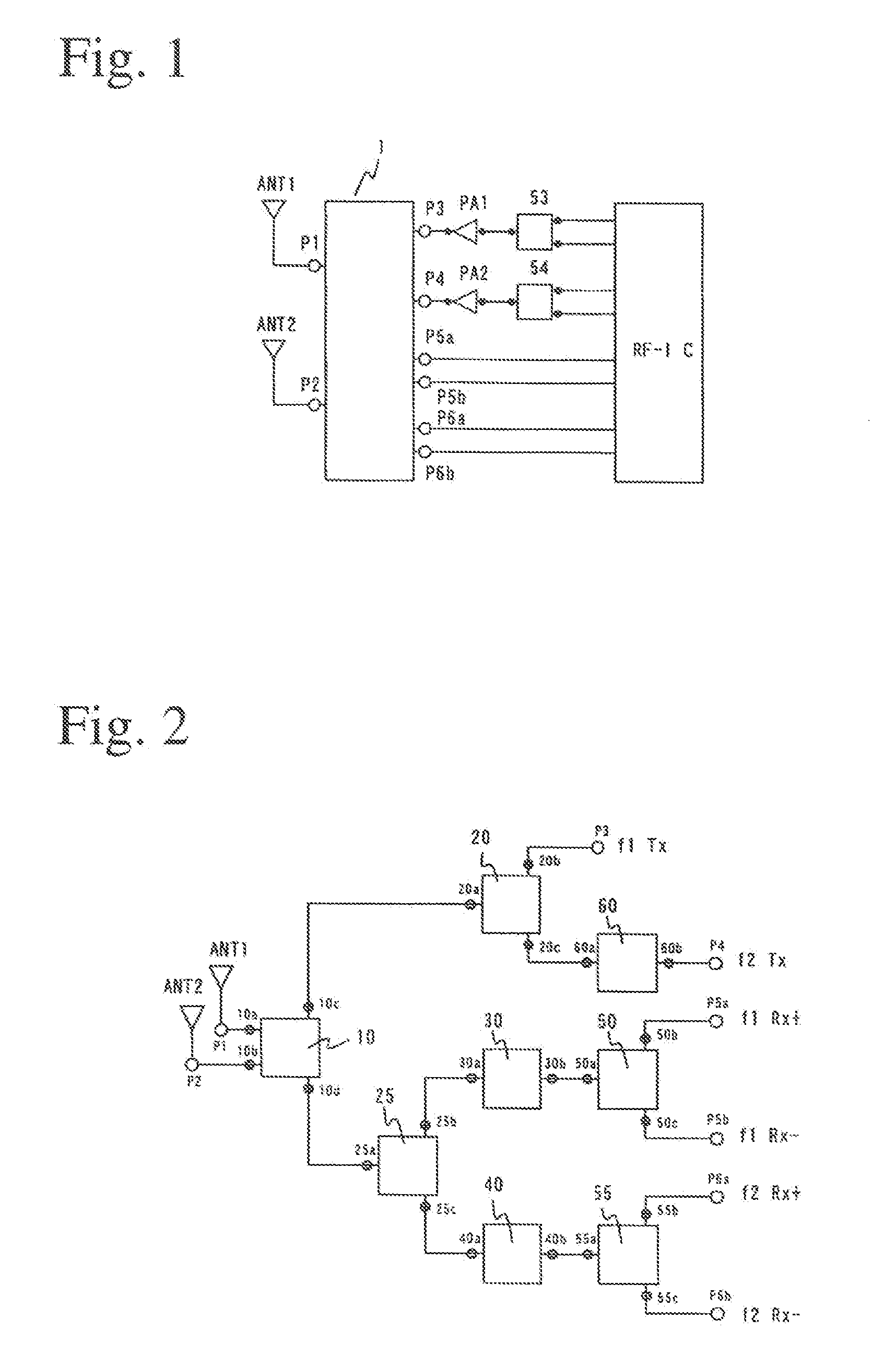
[0074]FIG. 1 shows the circuit of the multi-band communication apparatus according to a preferred embodiment of the present invention. This multi-band communication apparatus comprises two multi-band antennas ANT1, ANT2 transmittable and receivable in a 2.4-GHz band and a 5-GHz-band; a high-frequency switch 1 or a high-frequency circuit 1 comprising pluralities of diplexer circuits for switching the connection of the multi-band antennas and the transmitting circuits and receiving circuits; a transmitting / receiving circuit RF-IC comprising a transmitting / receiving means of IEEE802.11a and a transmitting / receiving means of IEEE802.11b for modulating transmission data and demodulating receiving data in each communication system, a switch circuit controller for controlling the switching of the high-frequency switch, and amplifiers for receiving signals; balanced-to-unbalanced converters 53, 54 for converting balanced signals to unbalanced signals; and amplifiers PA1, PA2 for transmissio...

embodiment 2

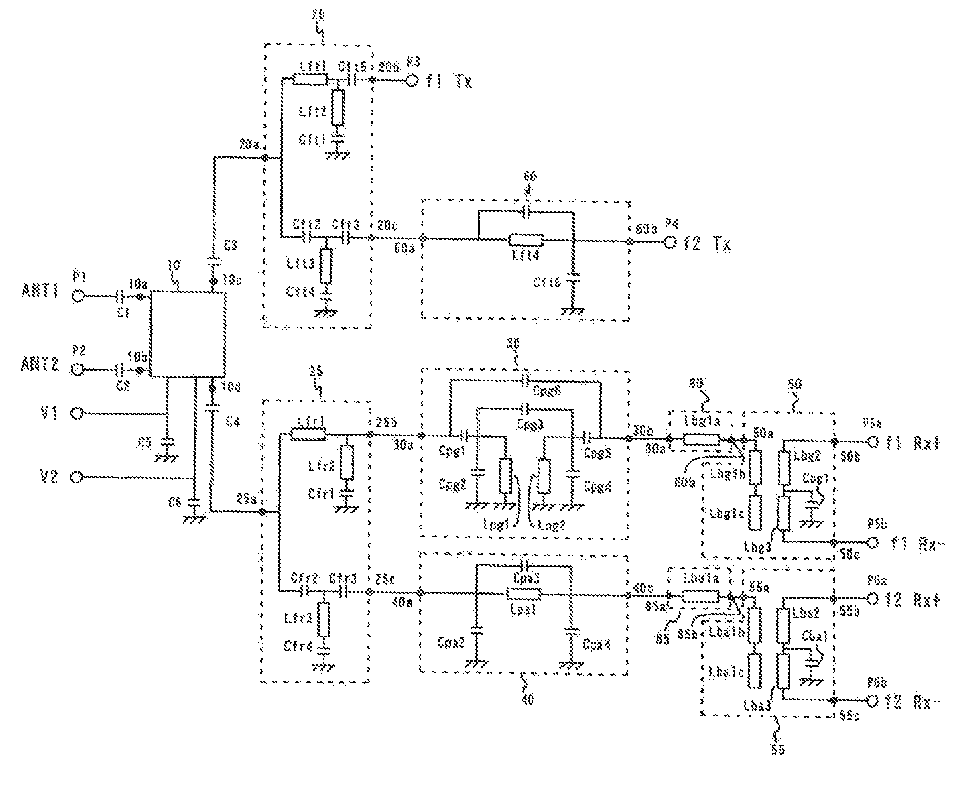
[0101] An example of the multi-band high-frequency circuit having the equivalent circuit shown in FIG. 3 formed in a laminate is shown in FIGS. 26-28. FIG. 26 shows the appearance of a multi-band high-frequency circuit component comprising first and second diplexer circuits 20, 25, filter circuits 30, 40, 60, first and second balanced-unbalanced circuits 50, 60, etc. in and on a laminate. FIGS. 27 and 28 show the structure of each layer in the laminate 100 constituting the high-frequency circuit component.

[0102] The laminate 100 is produced by laminating pluralities of ceramic green sheets as thick as 10-200 μm and made of, for instance, a dielectric ceramic sinterable at as low a temperature as 1000° C. or lower, each of which is provided with an electrode pattern formed by printing a conductive paste of Ag, Cu, etc., and integrally sintering them.

[0103] A lowermost green sheet 15 is covered with a ground electrode GND on its front surface, and provided with terminal electrodes f...

embodiment 3

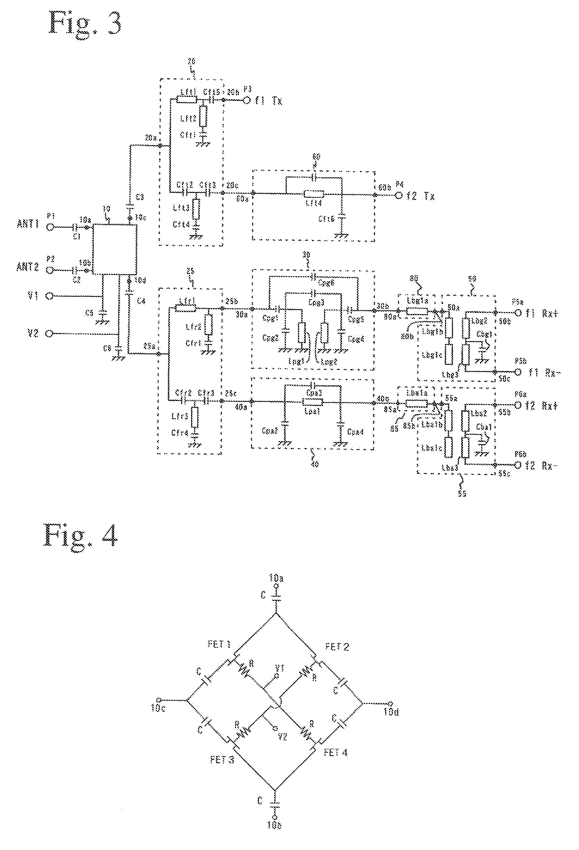
[0109]FIG. 29 shows the equivalent circuit of another multi-band high-frequency circuit. The feature of this multi-band high-frequency circuit is that the lower-frequency filter circuit in the second diplexer circuit 25 is constituted by a phase circuit Lfr1 and a bandpass filter circuit 30 having a 2.4-GHz passband. The phase circuit Lfr1 properly adjust the phase of a high-frequency signal, so that when viewed from the high-frequency switch circuit, the bandpass filter circuit 30 has high impedance in a band of 5 GHz, thereby preventing a 5-GHz-band, high-frequency signal from leaking to the receiving circuit in a 2.4-GHz band. In this embodiment, with the phase circuit Lfr1 constituted by transmission lines, the multi-band high-frequency circuit can be constituted by small numbers of circuit elements.


PUM


Abstract

A multi-band high-frequency circuit for performing wireless communications among pluralities of communication systems having different communication frequencies, comprising a high-frequency switch circuit comprising switching elements for switching the connection of pluralities of multi-band antennas to transmitting circuits and receiving circuits; a first diplexer circuit disposed between the high-frequency switch circuit and transmitting circuits for branching a high-frequency signal into frequency bands of the communication systems; a second diplexer circuit disposed between the high-frequency switch circuit and receiving circuits for branching a high-frequency signal into frequency bands of the communication systems; the first and second diplexer circuits each comprising a lower-frequency filter circuit and a higher-frequency filter circuit, a bandpass filter circuit being used as the lower-frequency filter circuit in the second diplexer circuit, or disposed between the lower-frequency filter circuit in the second diplexer circuit and the receiving circuit, so that there is a bandpass filter between the second diplexer circuit and a lower-frequency receiving circuit; the high-frequency switch circuit comprising first to fourth ports, the first port being connected to a first multi-band antenna, the second port being connected to a second multi-band antenna, the third port being connected to the first diplexer circuit, and the fourth port being connected to the second diplexer circuit; and the switching elements being controlled in an ON or OFF state to select a multi-band antenna for performing wireless communications and to switch the connection of the selected multi-band antenna to the transmitting circuit or the receiving circuit.

Description

FIELD OF THE INVENTION [0001] The present invention relates to a wireless communication apparatus for performing wireless transmission between electronic or electric equipments, particularly to a multi-band high-frequency circuit and a multi-band high-frequency circuit component commonly usable for at least two communication systems and capable of conducting diversity receiving, and a multi-band communication apparatus comprising such a multi-band high-frequency circuit component. BACKGROUND OF THE INVENTION [0002] Data communications by wireless LAN (WLAN) typically according to the IEEE802.11 standards are now widely used. They are used in personal computers (PCs); PC peripherals such as printers, hard disk drives, broadband rooters, etc.; electronic appliances such as facsimiles, refrigerators, standard-definition televisions (SDTVs), high-definition televisions (HDTVs), digital cameras, digital video recorders, cell phones, etc.; and as signal-transmitting means in place of wire...

Claims


Application Information

Patent Timeline
Patent Type & Authority Applications(United States)
IPC IPC(8): H03H7/46H04B1/00H04B1/40
CPCH04B1/0057H04B1/44
Inventor KEMMOCHI, SHIGERUFUKAMACHI, KEISUKEHAGIWARA, KAZUHIROUCHIDA, MASAYUKI
Owner MURATA MFG CO LTD
Why Eureka
Try Eureka