

Imaging unit and image sensor
a technology of image sensor and image, applied in the direction of color signal processing circuit, television system scanning details, television system, etc., can solve the problems of low photoelectric conversion amount per pixel, difficult to form a high-quality image, and high pixel density image, so as to prevent or suppress image degradation of photographic image
- Summary
- Abstract
- Description
- Claims
- Application Information
AI Technical Summary
Benefits of technology
Problems solved by technology
Method used
Image

Examples
embodiment 1-1
(Embodiment 1-1)
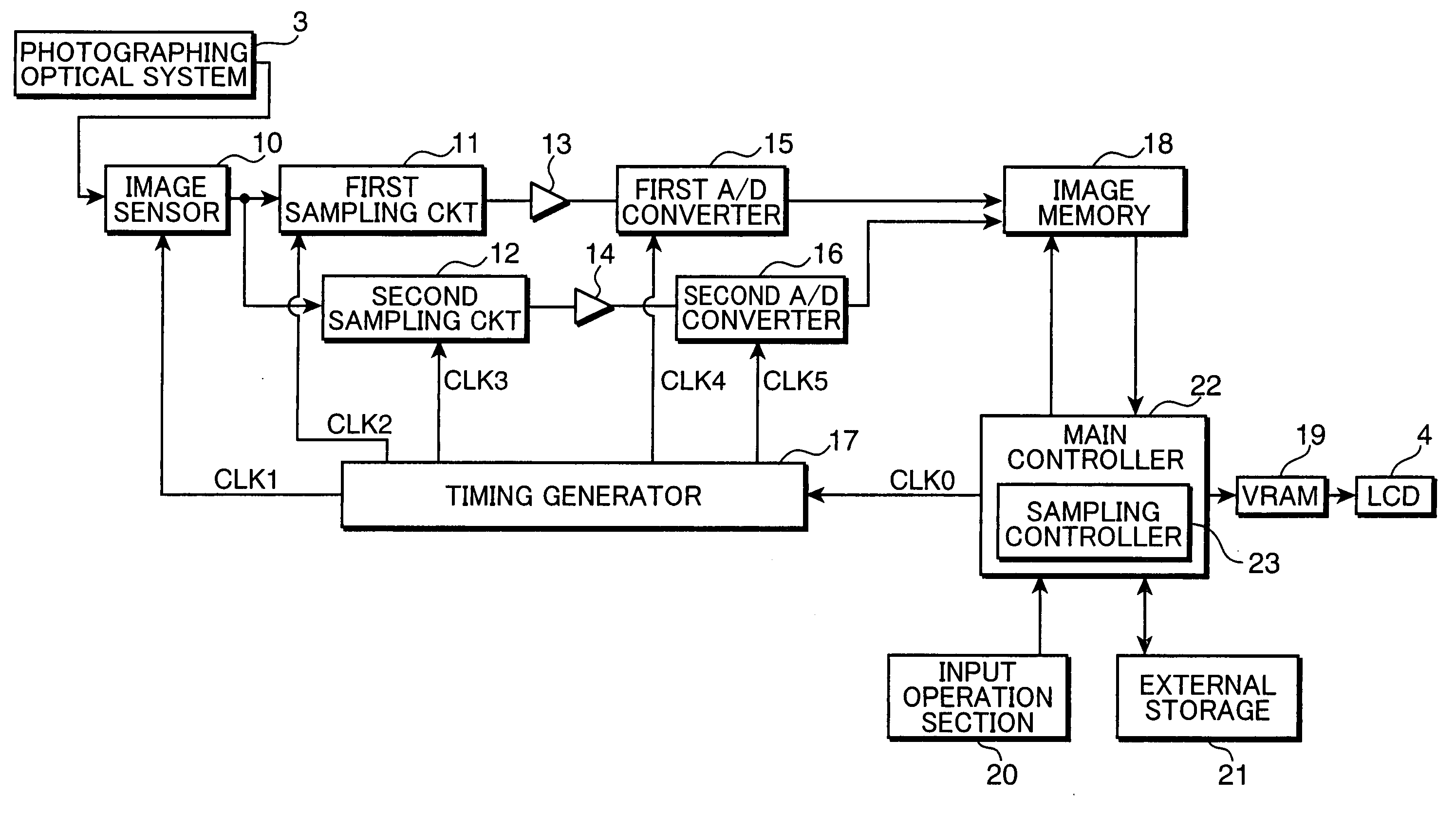
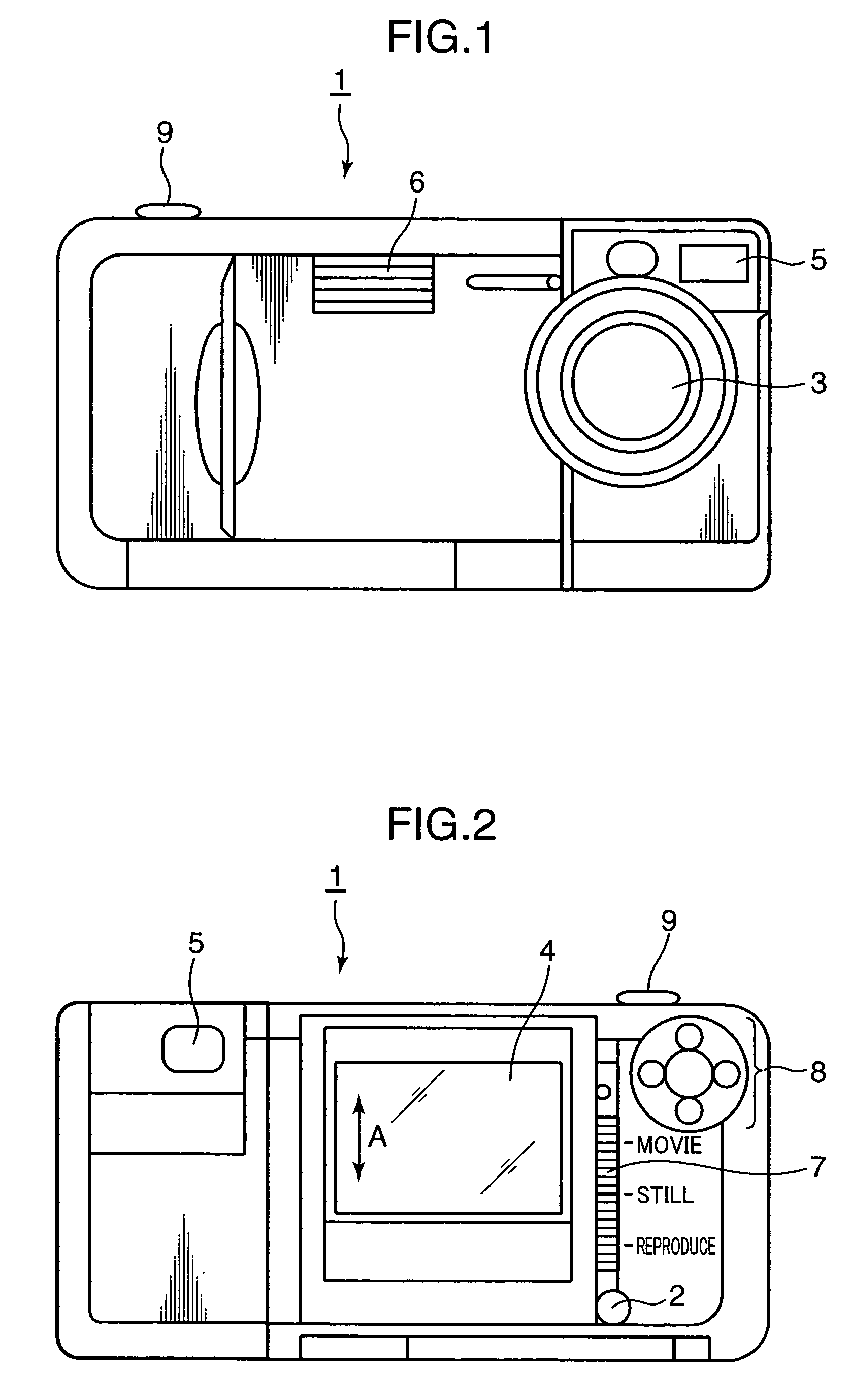
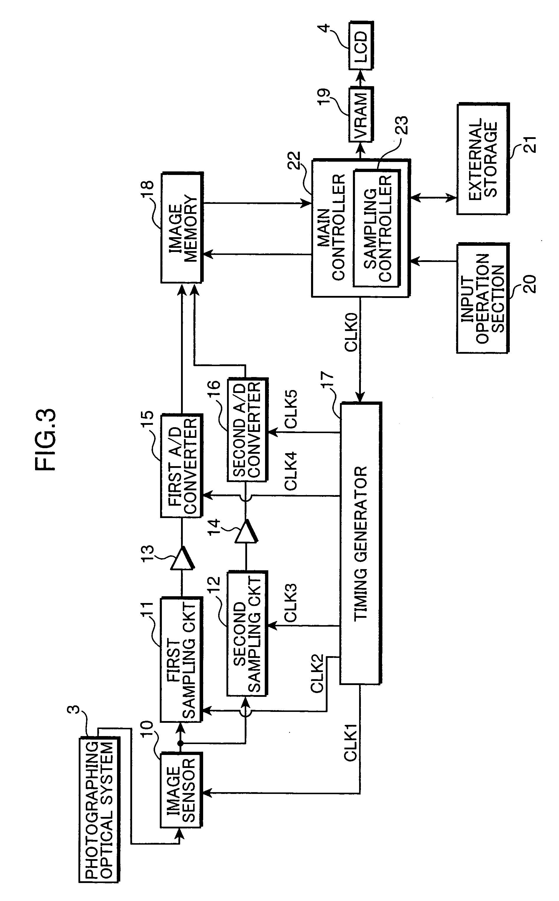
[0058]FIG. 1 is a front view of an image sensing apparatus 1 to which the invention is applied, and FIG. 2 is a rear view of the image sensing apparatus 1. As shown in FIGS. 1 and 2, the image sensing apparatus 1 includes a power source button 2, a photographing optical system 3, an LCD (Liquid Crystal Display) 4, an optical viewfinder 5, a built-in flash 6, a mode setting switch 7, a quadruple switch 8, and a shutter button 9.
[0059] The power source button 2 is adapted to switch over the power of the image sensing apparatus 1 between on-state and off-state. The photographing optical system 3 includes a zoom lens and an unillustrated mechanical shutter, and is adapted to form an optical image of an object onto an imaging surface of an image sensor 10 (see FIG. 3) such as a CCD (Charge Coupled Device) sensor.
[0060] The LCD 4 is adapted to display a live-view image or an image to be recorded in an external storage 21 (see FIG. 3), or to reproduce and display the imag...
embodiment 1-2
(Embodiment 1-2)
[0099] The embodiment 1-1is constructed in such a manner that after the first and the second sampling circuits 11 and 12 read out substantially all the pixel signals to be outputted from the image sensor 10, the first and the second sampling circuits 11 and 12 selectively sample the pixel signals. Alternatively, pixel signals may be outputted to individual output sections in outputting the pixel signals from an image sensor. FIG. 9 is a block diagram showing an electrical configuration of an image sensing apparatus 1 in the embodiment 1-2. Elements in the embodiment 1-2 which are substantially identical or equivalent to those in the embodiment 1-1are denoted by the same reference numerals.
[0100] Similarly to the embodiment 1-1, as shown in FIG. 9, the image sensing apparatus 1 in this embodiment is provided with a first sampling circuit 11′ and a second sampling circuit 12′, and with a signal line L1 as a signal path from an image sensor 10′ to the first sampling ci...
embodiment 1-3
(Embodiment 1-3)
[0109] In the embodiments 1-1 and 1-2, the CCD sensor is used as the image sensor. Alternatively, a CMOS (Complementary Metal Oxide Semiconductor) sensor may be used. FIG. 12 is a diagram showing an electrical configuration of an image sensing apparatus 100 in this embodiment. Elements in FIG. 12 which are identical or equivalent to those in the embodiment 1-1 are indicated by the same reference numerals.
[0110] As shown in FIG. 12, an image sensor 101 of the image sensing apparatus 100 is a CMOS sensor. A pixel configuration of the CMOS sensor is described. FIG. 13 is a diagram showing the pixel configuration of the CMOS sensor.
[0111] As shown in FIG. 13, each pixel of the CMOS sensor has a photodiode 1011 serving as a photoelectric conversion device of performing a photoelectric conversion, and transistors Tr1 through Tr4. The transistor Tr1 has an input terminal connected to a power source Vcc, a control terminal connected to an unillustrated vertical register, a...
PUM
 Abstract
Description
Claims
Application Information