Transparent conductive laminate and touch panel

a technology which is applied in the field of transparent conductive laminate and touch panel, can solve the problems of low flexibility or workability, inability to use certain purposes, and low transparency, and achieve good bending properties, good scratch resistance, and suppress the effect of transmitted light coloration

Inactive Publication Date: 2008-06-26
NITTO DENKO CORP
View PDF2 Cites 37 Cited by
  • Summary
  • Abstract
  • Description
  • Claims
  • Application Information

AI Technical Summary

Benefits of technology

[0020]The transparent conductive laminate of the invention has two transparent dielectric thin films including the first and second transparent dielectric thin films between the transparent conductive thin film and the film substrate. Such a structure also has good scratch resistance and good bending properties. In addition, the first transparent dielectric thin film uses a high-refractive-index, high-resistance complex oxide having a specific content of a specific component and is formed by a dry process, as described above, so that coloration of transmitted light can be suppressed, the productivity can be high, and optical adjustment can be easily performed.
[0021]According to the invention, the transparent conductive laminate is also configured to include a transparent laminated base substrate that includes at least two transparent base films laminated with a transparent pressure-sensitive adhesive layer interposed therebetween and is provide on the side of the transparent film substrate where no transparent conductive film is provided. Such a structure can improve not only pen input durability but also surface pressure durability, for example, when the transparent conductive laminate is used for touch panels.
[0022]The pen input durability and surface pressure durability of the transparent conductive laminate are further improved, because the transparent conductive thin film is provided on the side of the film substrate with the transparent dielectric thin films interposed therebetween. Specifically, the dielectric thin films effectively serve as an undercoat layer of the transparent conductive thin film to improve in-plane durability.

Problems solved by technology

Since the base member of the conductive glass is made of glass, it has low flexibility or workability and cannot be used for certain purposes.
However, such conventional transparent conductive thin films using film substrates not only have the problem of low transparency due to high light reflectance of the thin film surface but also have the problem of low scratch resistance so that they can get scratched to have an increased electrical resistance or suffer from disconnection during use.
However, the above-mentioned transparent conductive thin films using film substrates have low tapping durability and thus have a problem in which they can form short-life touch panels.
According to JP-A No. 2002-326301, however, a mixture of organic and inorganic materials is used for the first transparent dielectric thin film formed on the transparent film substrate, and thus it is not easy to adjust optical properties such as transparency.
JP-A No. 2000-301648 discloses various methods for forming the first transparent dielectric thin film on the transparent film substrate, but none of the methods has a sufficient rate of film production.
However, the techniques disclosed in the patent literatures cannot achieve satisfactory pen input durability and thus can never achieve satisfactory surface pressure durability.

Method used


Image

  • Transparent conductive laminate and touch panel
  • Transparent conductive laminate and touch panel
  • Transparent conductive laminate and touch panel

Examples


example 1

Formation of First Transparent Dielectric Thin Film

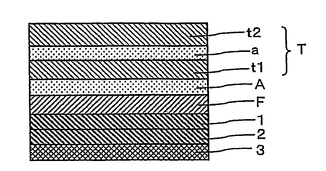
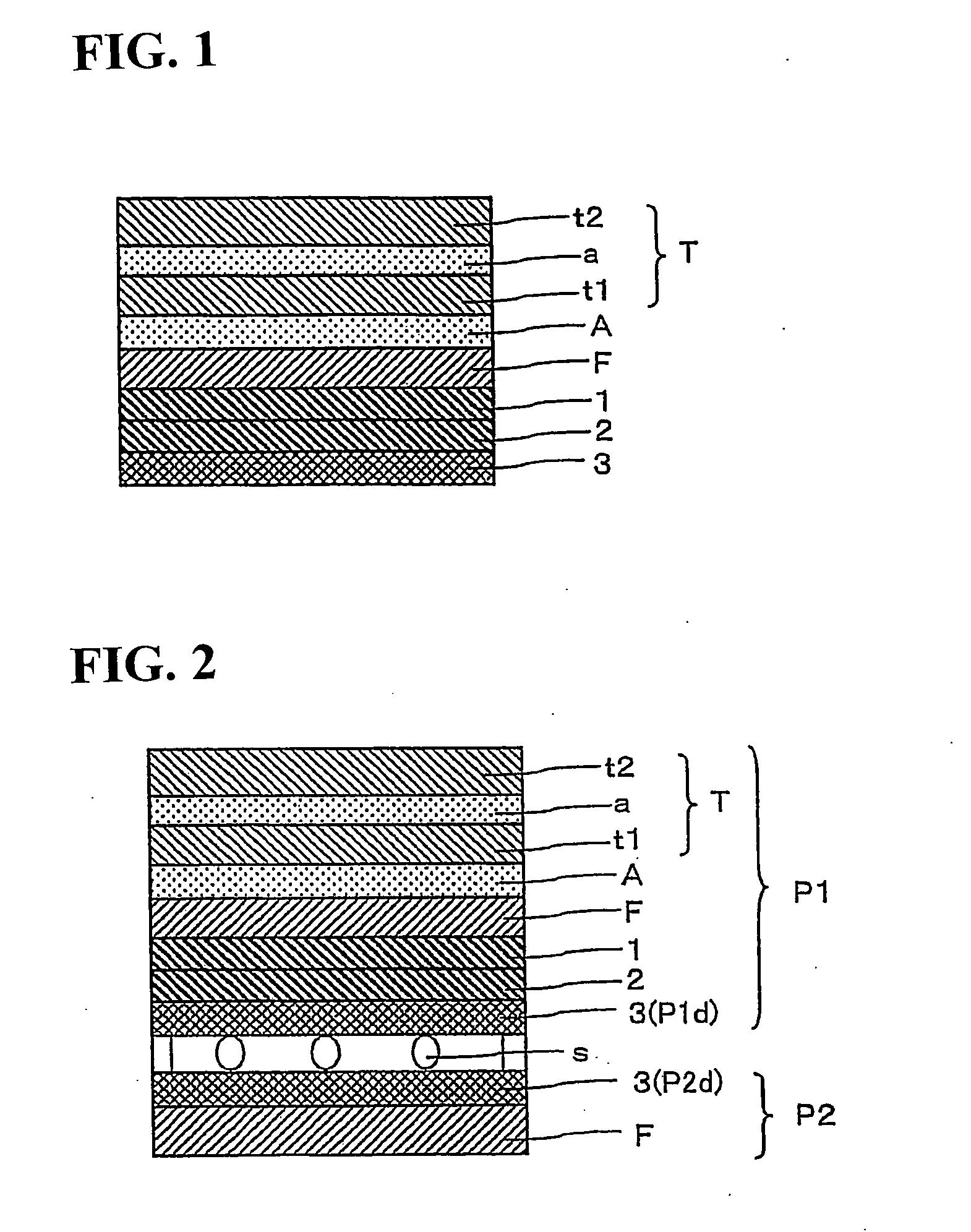
[0060]A first transparent dielectric thin film (with a light refractive index n1 of 2.1) of a complex oxide containing 100 parts of indium oxide, 10 parts of tin oxide and 25 parts of cerium oxide was formed by a reactive sputtering method under the conditions below in a mixed gas atmosphere of 95% argon gas and 5% oxygen gas from a sintered body of a mixture of 100 parts of indium oxide, 10 parts of tin oxide and 25 parts of cerium oxide on one side of a film substrate (with a light refractive index nf of 1.66) made of a 125 μm-thick polyethylene terephthalate film (hereinafter referred to as PET film). The first transparent dielectric thin film had a thickness of 32 nm and a surface resistance of 8.5×10⁹ Ω / square.

Sputtering Conditions

[0061]Target Size: 200 mm×500 mm[0062]Power: 3.0 kW[0063]Voltage: 450 V[0064]Discharge Time: 1 minute[0065]Degree of Vacuum: 0.5 Pa

Formation of Second Transparent Dielectric Thin Film

[0066]SiO2 (with ...

example 2

Formation of Second Transparent Dielectric Thin Film

[0072]A wet SiO2 film was formed on the same first transparent dielectric thin film as obtained in example 1 (see the section “Formation of First Transparent Dielectric Thin Film”) by a silica coating method. Specifically, a silica sol (Colcoat P, manufactured by Colcoat Co., Ltd.) was diluted with ethanol to a solid concentration of 2% and then applied to the first transparent dielectric thin film. The coating was dried at 150° C. for 2 minutes and then cured to form a 30 nm-thick wet SiO2 film (with a relative refractive index of 1.46).

Preparation of Transparent Conductive Laminate

[0073]A transparent conductive thin film was formed, and then a transparent conductive laminate was prepared, using the process of example 1, except that the second transparent dielectric thin film was formed by the above-described method.

example 3

Formation of First Transparent Dielectric Thin Film

[0074]A transparent hard-coat layer (with a light refractive index of 1.54) was formed on a 25 μm-thick PET film by a process including the steps of mixing 100 parts of an ultraviolet curable resin (KRX571-76NL manufactured by Asahi Denka Kogyo K.K.) and 0.5 parts of a silicone-based leveling agent and diluting them with a solvent so as to form a solution with a solids content of 20%, applying the solution with a No. 16 wire bar such that the film would have a thickness of 3 μm after drying, vaporizing the solvent with a drying oven, and then curing the coating by application of ultraviolet light from a high pressure mercury lamp.

[0075]A first transparent dielectric thin film was formed using the process of example 1, except that the PET film provided with the hard-coat layer was used as the film substrate and that a sintered body of a mixture of 100 parts of indium oxide, 5 parts of tin oxide and 10 parts of cerium oxide was used i...


PUM

PropertyMeasurementUnit
thicknessaaaaaaaaaa
thicknessaaaaaaaaaa
refractive indexaaaaaaaaaa

Abstract

A transparent conductive laminate includes: a first transparent dielectric thin film; a second transparent dielectric thin film; a transparent conductive thin film; a transparent film substrate having a thickness of 2 μm to 200 μm, and the first transparent dielectric thin film, the second transparent dielectric thin film, and the transparent conductive thin film formed on one side of the substrate in this order; a transparent pressure-sensitive adhesive layer; and a transparent base substrate bonded to another side of the transparent film substrate with a transparent pressure-sensitive adhesive layer interposed therebetween, wherein the first transparent dielectric thin film is formed by vacuum deposition, sputtering or ion plating and comprises a complex oxide containing 100 parts by weight of indium oxide, 0 to 20 parts by weight of tin oxide and 10 to 40 parts by weight of cerium oxide, a refractive index n1 of the first transparent dielectric thin film, a refractive index n2 of the second transparent dielectric thin film, and a refractive index n3 of the transparent conductive thin film satisfy a relationship: n2<n3≦n1, and the transparent base substrate is a transparent laminated base substrate having at least two transparent base films that are laminated with the transparent pressure-sensitive adhesive layer interposed therebetween.

Description

BACKGROUND OF THE INVENTION[0001]1. Field of the Invention[0002]The present invention relates to a transparent conductive laminate including a film substrate and a conductive thin film provided on the film substrate and having transparency in the visible light range. The transparent conductive laminate of the invention may be used for transparent electrodes in advanced display systems, such as liquid crystal displays and electroluminescence displays, and touch panels, and also used for prevention of static charge of transparent products or electromagnetic wave shielding.[0003]2. Description of the Related Art[0004]Concerning conventional transparent conductive thin films, the so-called conductive glass is well known, in which an indium oxide thin film is formed on a glass member. Since the base member of the conductive glass is made of glass, it has low flexibility or workability and cannot be used for certain purposes. In recent years, therefore, transparent conductive films using ...

Claims


Application Information

Patent Timeline
Patent Type & Authority Applications(United States)
IPC IPC(8): B32B7/02
CPCY10T428/24942C23C14/08B32B7/025
Inventor NASHIKI, TOMOTAKESUGAWARA, HIDEO
Owner NITTO DENKO CORP
Why Eureka
Try Eureka