Refresh-free dynamic semiconductor memory device

a dynamic semiconductor and memory device technology, applied in static storage, information storage, digital storage, etc., can solve the problems of increased junction leakage current, increased leakage current through capacitor insulating film, and rise in read error for h data, etc., to achieve low power consumption

Inactive Publication Date: 2005-08-02
RENESAS ELECTRONICS CORP
View PDF9 Cites 36 Cited by
  • Summary
  • Abstract
  • Description
  • Claims
  • Application Information

AI Technical Summary

Benefits of technology

[0040]It is an object of the present invention to provide a semiconductor memory device capable of achieving low power consumption.

Problems solved by technology

That is, after the time T1 elapses, the sense amplifier malfunctions, read error for H data arises in which H level data may be amplified into L level data.
Hence, a thermal budget (a product of time and temperature in an annealing process) in a high temperature processing applied in formation of the memory capacitor is reduced For this reason, an impurity region and an insulating film cannot be subject to a thermal process at a prescribed temperature for a sufficient time, resulting in an increased junction leakage current and in an increased leakage current through a capacitor insulating film, although by a small amount.
Such a step cannot be perfectly eliminated even when an interlayer insulating film between interconnection lines is planarized to some extent by a CMP (a chemical mechanical polishing) process.
Accordingly, a pitch of metal interconnection lines cannot be reduced sufficiently because of irregular reflection and others at steps in an exposure process of a photolithographic process.
Hence, a metal interconnection line pitch required for a high density library of a logic is difficult to be achieved.
In addition, a power supply line of the embedded DRAM section and the substrate are apt to be affected by noise due to a high speed operation of the logic section.
Refresh characteristics of the embedded DRAM are deteriorated as compared with a general purpose DRAM by these various factors in the fabrication process or a chip operation.
Moreover, during operation, a refresh time of an embedded DRAM is required to be short as compared with a general purpose DRAM, thereby increasing a current consumed for data holding.
Especially, in a case where a system LSI with an embedded DRAM is applied in products such as a portable information equipment and digital camera driven by a battery, a power consumption is a more predominant factor than increase in storage capacity.
Accordingly, increase in consumed current associated with poor refresh characteristics is a serious problem against application to a battery driven equipment.

Method used


Image

  • Refresh-free dynamic semiconductor memory device
  • Refresh-free dynamic semiconductor memory device
  • Refresh-free dynamic semiconductor memory device

Examples


first embodiment

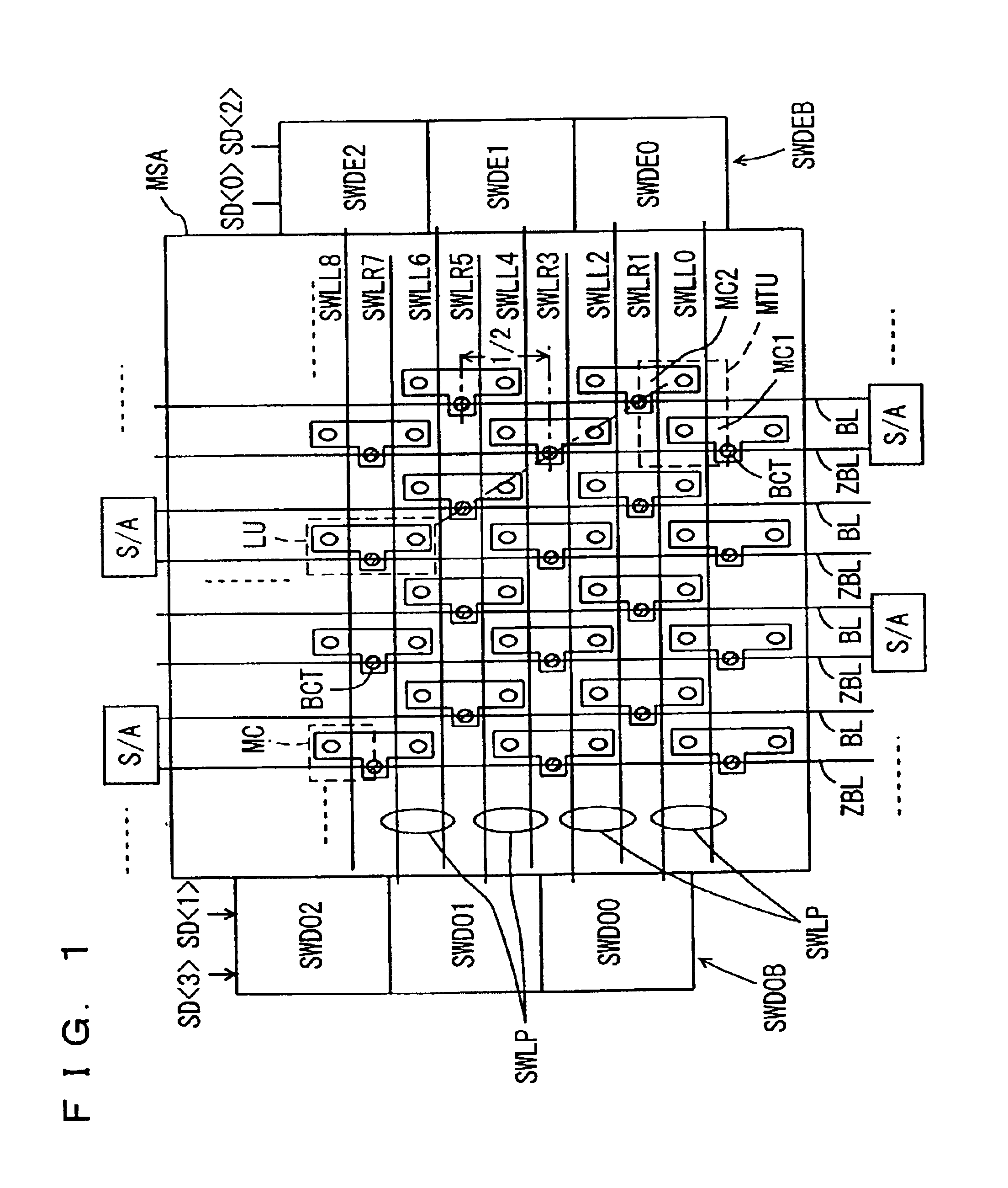
[0160]FIG. 1 is a diagram schematically showing an array section of a semiconductor memory device according to a first embodiment of the present invention. In FIG. 1, memory cells MC are arranged such that memory cells adjacent in the column direction share a bit line contact BCT. One layout unit LU is constituted of two memory cells MC sharing the bit line contact BCT. The layout units LU are placed such that in the column direction arrangement, layout units are laid out every second column, while in the row direction arrangement, layout units are laid out every third row. With respect to bit line contacts BCT, accordingly, the bit line contacts BCT are laid out every fifth row in alignment along the column direction, while the bit line contacts BCT are laid out every second column in alignment along the row direction. In the row direction, the layout units LU are arranged being sifted by one column. A length of a projection of a minimum pitch of memory cells MC on an oblique line ...

second modification

[0254]FIG. 25 is a diagram schematically showing a configuration of the self-refresh timer 9 according to a second modification of the first embodiment of the present invention. In FIG. 25, the refresh timer 9 includes: a variable ring oscillator 9j started, when the sleep mode instructing signal SLEEP_MODE is activated, to perform an oscillating operation; and a counter 9k counting output signals of the variable ring oscillator 9j and issuing a refresh request signal FAY when a count value reaches a prescribe value. The number of stages of the variable ring oscillator 9j is made smaller to shorten an oscillating cycle when the twin-cell write mode instructing signal TWC_WRITE_MODE is activated. In the twin-cell write mode, there is a need to write data stored once in the one bit / one cell mode into one bit / two cell mode unit cells. Therefore, a data hold time in the twin-cell write mode is determined by a refresh time for memory cells in the one bit / one cell mode.

[0255]For example, ...

second embodiment

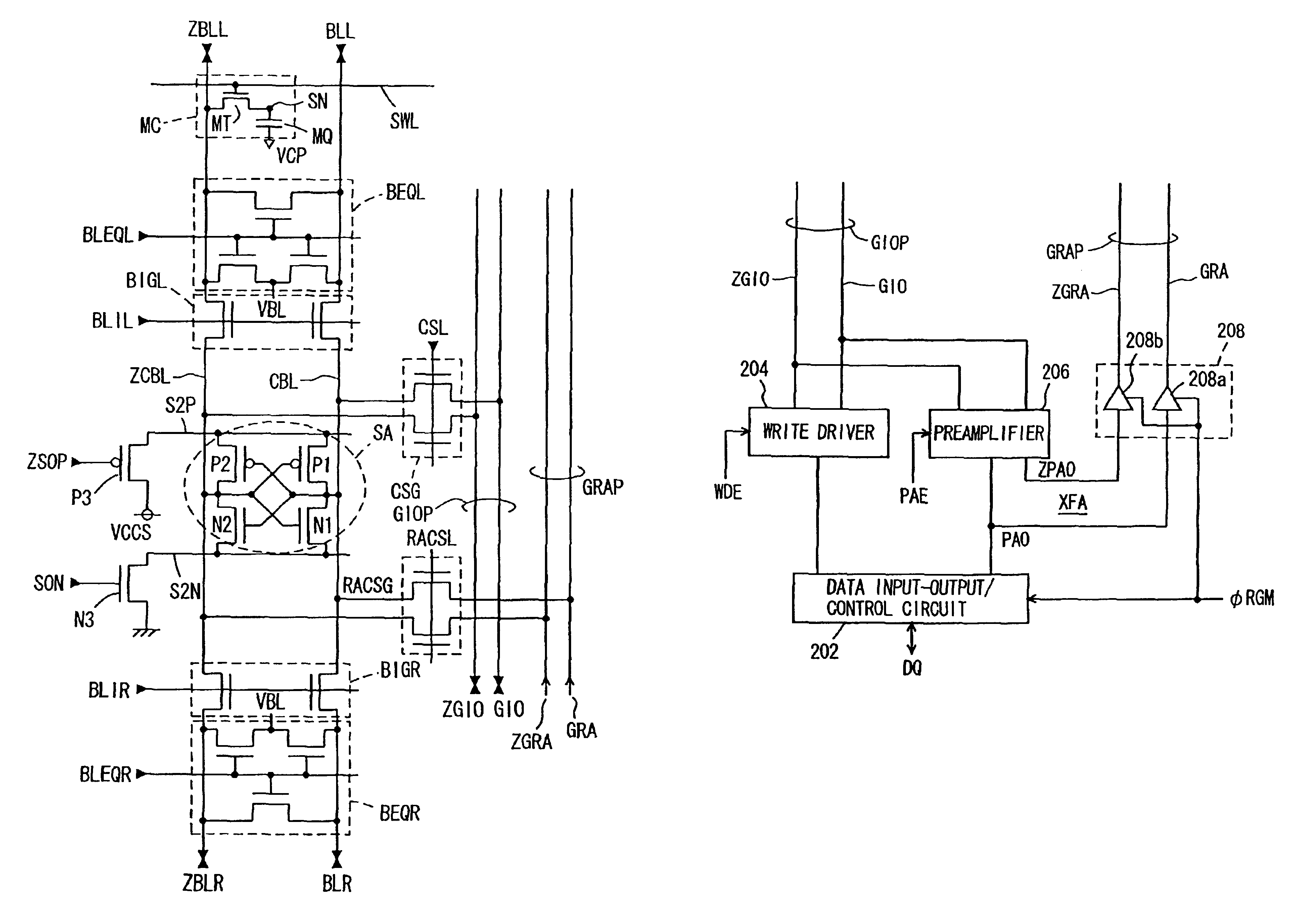
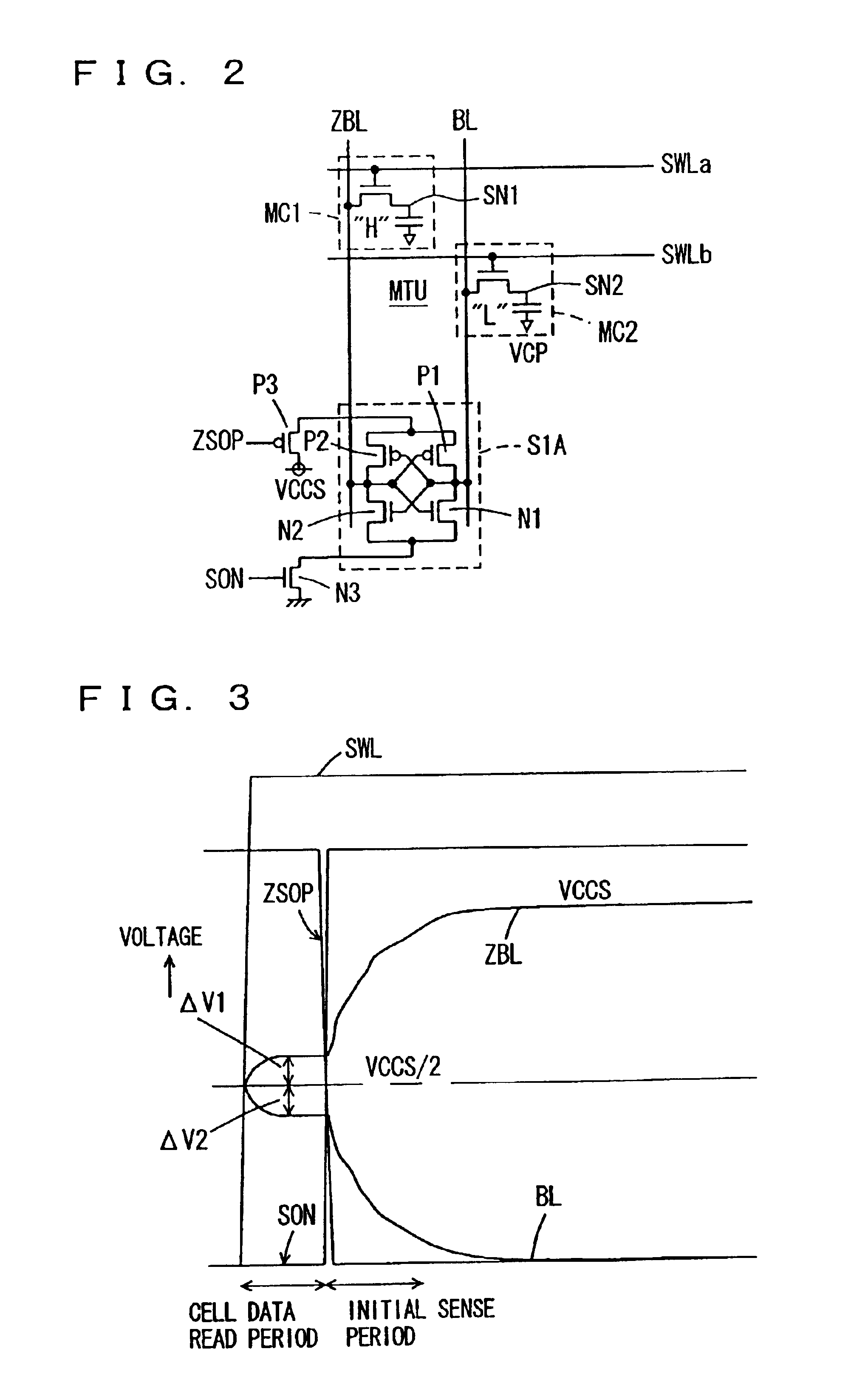
[0258]FIG. 26 is a diagram representing a configuration of a main part of a semiconductor memory device according to a second embodiment of the present invention. In FIG. 26, a configuration of a part associated with one sense amplifier SA is shown. The sense amplifier SA is coupled with bit lines BLL and ZBLL of one memory cell sub array through a bit line isolation gate BIGL, and is coupled with bit lines BLR and ZBLR of another memory cell sub array through a bit line isolation gate BIGR. The sense amplifier SA includes: a pair of cross-coupled P channel MOS transistors P1 and P2; and a pair of cross-coupled N channel MOS transistors N1 and N2. The P channel MOS transistors P1 and P2 drive a bit line at a higher potential of common bit lines CBL and ZCBL to the array power supply voltage VCCS level. The N channel MOS transistors N1 and N2 drive a bit line at a lower potential of the common bit lines CBL and ZCBL to the ground voltage level.

[0259]Sense drive circuits SDK are provi...


PUM


Abstract

In a data holding mode, data storage in a one bit/one cell scheme in a normal operating mode are rearranged into data storage in a twin-cell mode in which data are stored in a one bit/two cell scheme. In the twin-cell mode, two sub word lines are simultaneously driven into a selected state, and storage data of memory cells are read out on both of bit lines in a pair, to perform a sense operation. Thus, the read-out voltage can be increased to improve the data retention characteristics for lengthening a refresh interval, resulting in a reduced power consumption in the data holding mode.

Description

[0001]This application is a divisional of application Ser. No. 09 / 817,177, filed Mar. 27, 2001 now U.S. Pat. No. 6,449,204.BACKGROUND OF THE INVENTION[0002]1. Field of the Invention[0003]The present invention relates to a semiconductor memory device and particularly, to a configuration for reducing power consumption of a semiconductor memory device. More particularly, the present invention relates to a configuration for reducing power consumption of an embedded type DRAM (dynamic random access memory) used in a system LSI.[0004]2. Description of the Background Art[0005]In a system LSI constituted of DRAM and a logic such as a processor, ASIC (application specific integrated circuit) or the like in a merged manner, DRAM and the logic are interconnected to each other using an internal data bus of multiple bits such as 128 bits to 512 bits. This internal data bus is on-chip interconnection lines, and a parasitic capacitance and a parasitic resistance thereof are small as compared with ...

Claims


Application Information

Patent Timeline
Patent Type & Authority Patents(United States)
IPC IPC(8): G11C11/408G11C7/10G11C11/406G11C11/407G11C11/401G11C11/403G11C11/405G11C11/409G11C29/02G11C29/04G11C29/14
CPCG11C7/1045G11C11/406G11C11/4087G11C29/006G11C29/02G11C29/021G11C29/028G11C29/50G11C29/50012G11C29/50016G11C2211/5641G11C29/83G11C2029/1204G11C2207/104G11C2211/4013G11C11/401
Inventor ARIMOTO, KAZUTAMISHIMANO, HIROKIFUJINO, TAKESHIHASHIZUME, TAKESHI
Owner RENESAS ELECTRONICS CORP
Why Eureka
Try Eureka