Electrochemical double-layer capacitor using organosilicon electrolytes
a technology of organosilicon and capacitor, which is applied in the direction of liquid electrolytic capacitor, electrochemical generator, etc., can solve the problems of inability to deliver high-power pulses, inability to stabilize at the operating voltage, and hazardous flammable and toxic materials such as acetonitrile, etc., to achieve stable storage and processing, easy to make, and high yield
- Summary
- Abstract
- Description
- Claims
- Application Information
AI Technical Summary
Benefits of technology
Problems solved by technology
Method used
Image
Examples
example 1
[0085] In this example an EDLC device was fabricated from activated carbon nanotubes deposited on stainless steel current collectors, using solid cross-linked organosiloxane polymer as the electrolyte, separator and as a binder.
[0086] Fabrication of the device began with preparation of the electrode / current collector assembly plates from activated carbon nanotubes powder. The multi-walled carbon nanotubes (MWCNTs) used for this study were produced by chemical vapor deposition and treated with hydrochloric acid at room temperature to extract catalyst and other impurities. The nanotubes powder then was washed with distilled water and dried.
[0087] Purified MWCNTs were refluxed with concentrated boiling nitric acid for about 10 hours for activation, and then washed with distilled water followed by rinsing with ethanol and drying in vacuum 10−3 mmHg at 60° C. Activated nanotubes then were dispersed by ultrasound sonication for 30 min in dimethylformamide (DMF) to prepare a colloidal su...
example 2
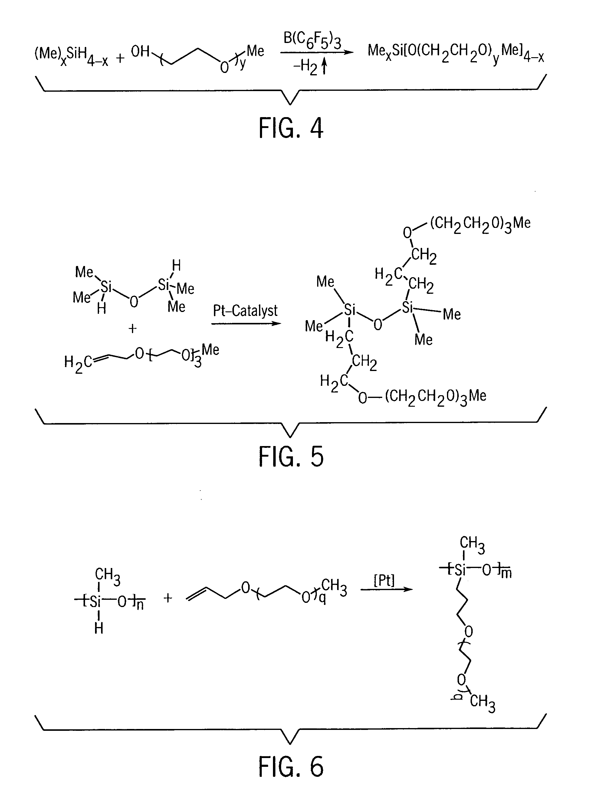
[0094] An electric double layer capacitor was prepared in the same manner as in Example 1, except that vertically aligned carbon nanofibers were used as a high surface area carbonaceous component of the electrode material (for two electrodes) instead of activated carbon nanotubes. We used a 0.8M solution of LiBOB in liquid disiloxane of FIG. 5 as the electrolyte, and used a PE / PP / PE tri-layer film (Celgard 3501, 25 μm) as a conventional separator.
[0095] Vertically aligned carbon nanofibers were grown on titanium / nickel coated stainless steel substrates using DC plasma-enhanced chemical vapor deposition. Typical growth conditions used flow rates of 80 standard cubic centimeters per minute (sccm) ammonia and 30 sccm acetylene, with a chamber pressure of 4 Torr and a DC power of 360 watts. Each metal layer in Ti / Ni coating had 50 nm thickness.
[0096] A two-electrode assembly, containing arrayed nanofiber electrodes of this example, was then placed into the Teflon Swagelok electrochemi...
example 3
[0097] Attention is called to FIG. 10 where there is shown an alternative monolithic nanofiber based EDLC. There is shown a substrate 30 preferably made of silicon nitride. The substrate is then coated with a thin layer of molybdenum 31, which is in turn coated with a thin layer of titanium 32. Spaced strips of nickel 33 / 34 are then positioned along the structure.
[0098] Vertically aligned carbon nanofibers 35 were then grown on the nickel lines using DC plasma-enhanced chemical vapor deposition. The growth conditions we used were the same as in Example 2.
[0099] In this example, our most preferred form nanofibers were grown on silicon nitride substrates that we covered with a thin film consisting of 50 nm Mo, followed by 20 nm Ti, and finally 20 nm Ni as the top layer strips. SEM images (see FIG. 11) show that the nanofibers were vertically aligned with an average diameter of˜75 nm. The length of the nanofibers was controlled by varying the duration of the growth. Nanofibers used f...
PUM
 Abstract
Description
Claims
Application Information


