Semiconductor storage device

a storage device and semiconductor technology, applied in static storage, digital storage, instruments, etc., can solve the problems of increasing the scale of the circuitry operating in the output buffer circuit, increasing the latency of the ca, and increasing the unnecessary circuitry for data storage, so as to reduce the unnecessary circuitry

Active Publication Date: 2007-04-05
MICRON TECH INC
View PDF2 Cites 22 Cited by
  • Summary
  • Abstract
  • Description
  • Claims
  • Application Information

AI Technical Summary

Benefits of technology

[0008] An object of the present invention is to provide a semiconductor storage device which enables the number of bits of latch circuits included in the output buffer circuit to be selectively switched when operating conditions change depending on the frequency of the external clock or the like, and can reduce unnecessary circuitry to prevent an increase in consumption current during high-speed access, while ensuring a reliable operation during low-speed access.
[0010] According to the semiconductor storage device of the present invention, when a read command is issued, L bits of data prefetched from the memory array is transferred in parallel to the output buffer circuit through the internal bus and is serially transferred to the outside through either the M-bit latch circuit or the N-bit latch circuit. Since the parallel transfer of the L bits through the internal bus shifts to the serial transfer each of 1 bit to the outside, the transfer speed of the internal bus requires only 1 / L-th of that of the external transfer speed. In this case, in the output buffer circuit in which the transfer data is stored, the M-bit latch circuit and the N-bit latch circuit can be switched in accordance with operating conditions. Therefore, when using a small scale M-bit latch, it is possible to reduce consumption current during the burst read operation, and when using the N-bit latch circuit capable of storing a larger number of bits, it is possible to reliably prevent malfunction caused by a change in the access time or the like.
[0014] By such a configuration, when the access time is reduced using a high-speed clock, the path of the M-bit circuit having a small circuit scale is set to reduce consumption current, and when the access time is increased using a low-speed clock, the path of the N-bit circuit capable of storing a large amount of data is set to prevent malfunction.
[0023] As described above, according to the present invention, a configuration can be realized in which L bits of prefetched data from the memory array is transferred in parallel to the internal bus, each bit of the data is stored in each FIFO buffer, each the stored data is extracted to be transferred serially to the outside in accordance with the input sequence, and each FIFO buffer is capable of switching selectively between paths of the N-bit latch circuit and the M-bit latch circuit. Accordingly, by the control in accordance with operating conditions of the semiconductor storage device, when the path of the M-bit latch circuit having a small circuit scale is selected, consumption current can be reduced, and when the path of the N-bit latch circuit capable of storing large size data is selected, an operating margin can be ensured to prevent malfunction. Further, by generating a determination signal based on the access time, the path of the M-bit latch circuit and the path of the N-bit latch circuit can be automatically switched, and thereby it is possible to achieve an optimum burst read operation.

Problems solved by technology

In recent years, due to rapid advances in speeding up the external clock, there is a tendency that the CAS latency increases.
Accordingly, when configuring the output buffer circuit which conforms the worst operating condition in which the external clock has a wide frequency range, unnecessary circuitry for data storage increases.
In this case, particularly when a high-speed external clock is used, the unnecessary circuitry in the output buffer circuit causes problems, such as an increase in the scale of circuitry operating in the output buffer circuit and an increase in the number of control-signal lines.
A combination of the factors described above causes a problem in that, particularly, current consumed during high-speed access to the DRAM increases.

Method used


Image

  • Semiconductor storage device
  • Semiconductor storage device
  • Semiconductor storage device

Examples


Embodiment Construction

[0038] An embodiment of the present invention will be described below with reference to the accompanying drawings. A case in which the present invention is applied to a DRAM, which serves as a semiconductor storage device, will be described in this embodiment. The present invention is effectively applied to a DRAM and more particularly to a DDR SDRAM which operates in synchronization with a rising edge and a falling edge of an external clock.

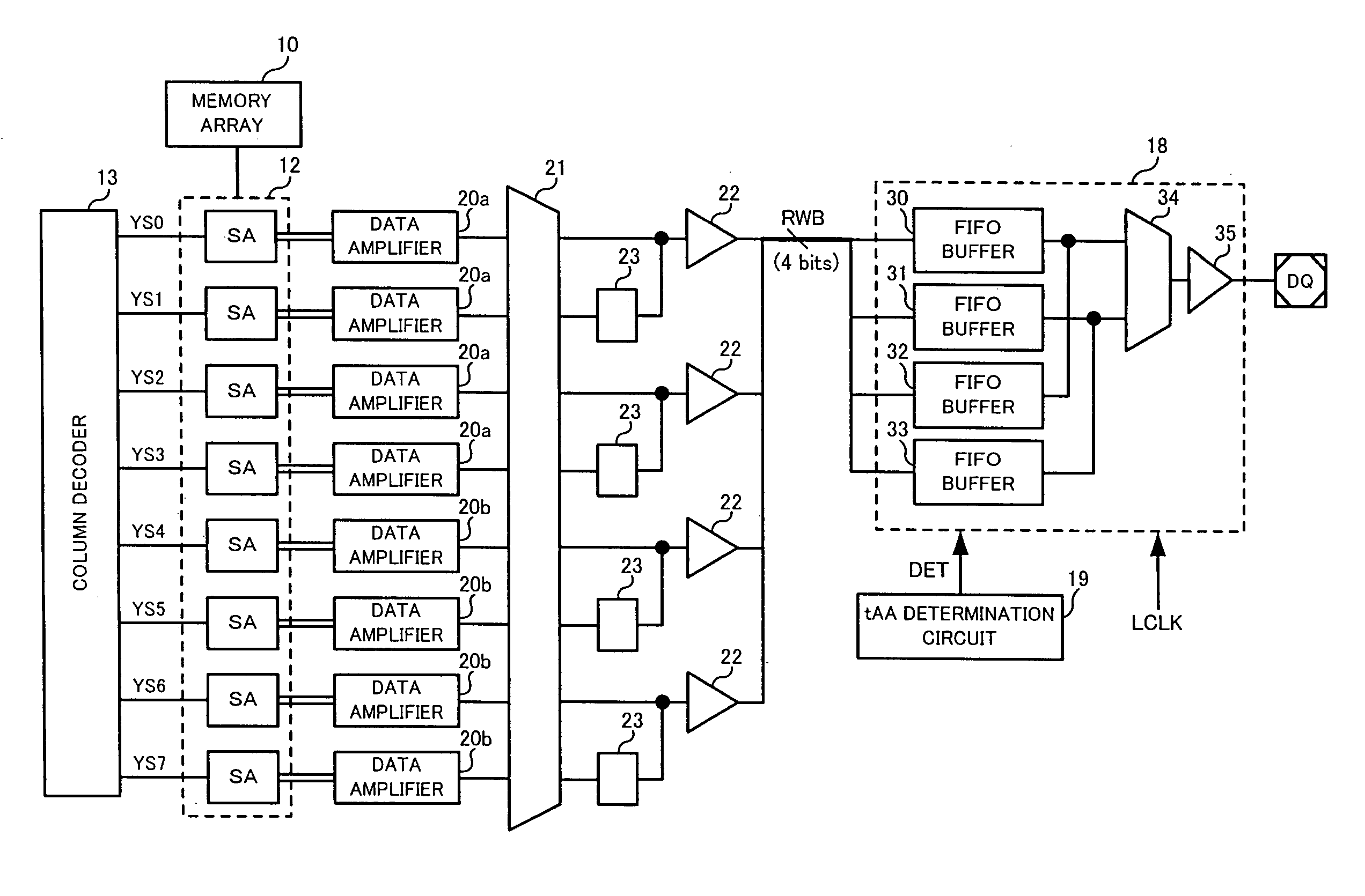
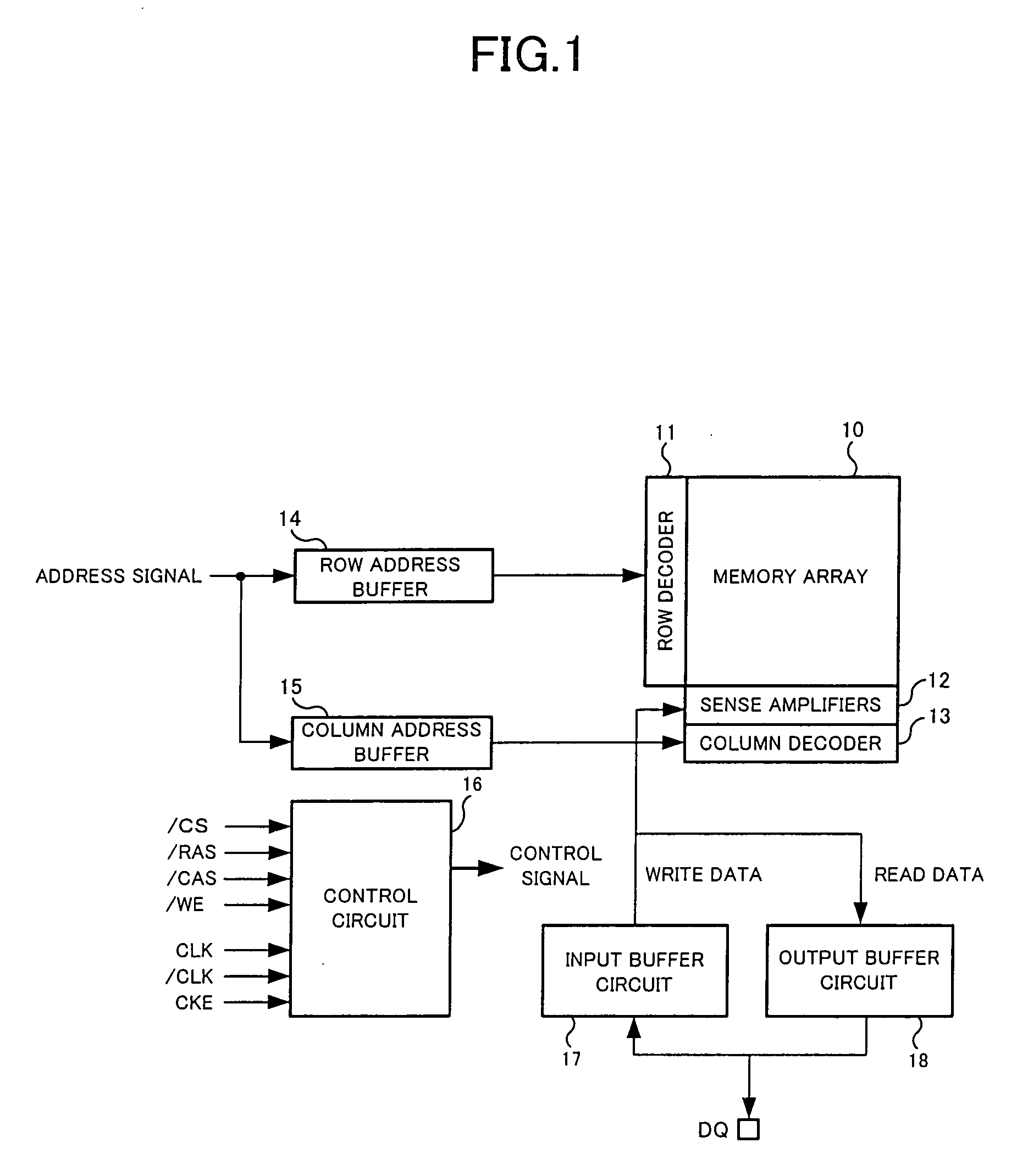
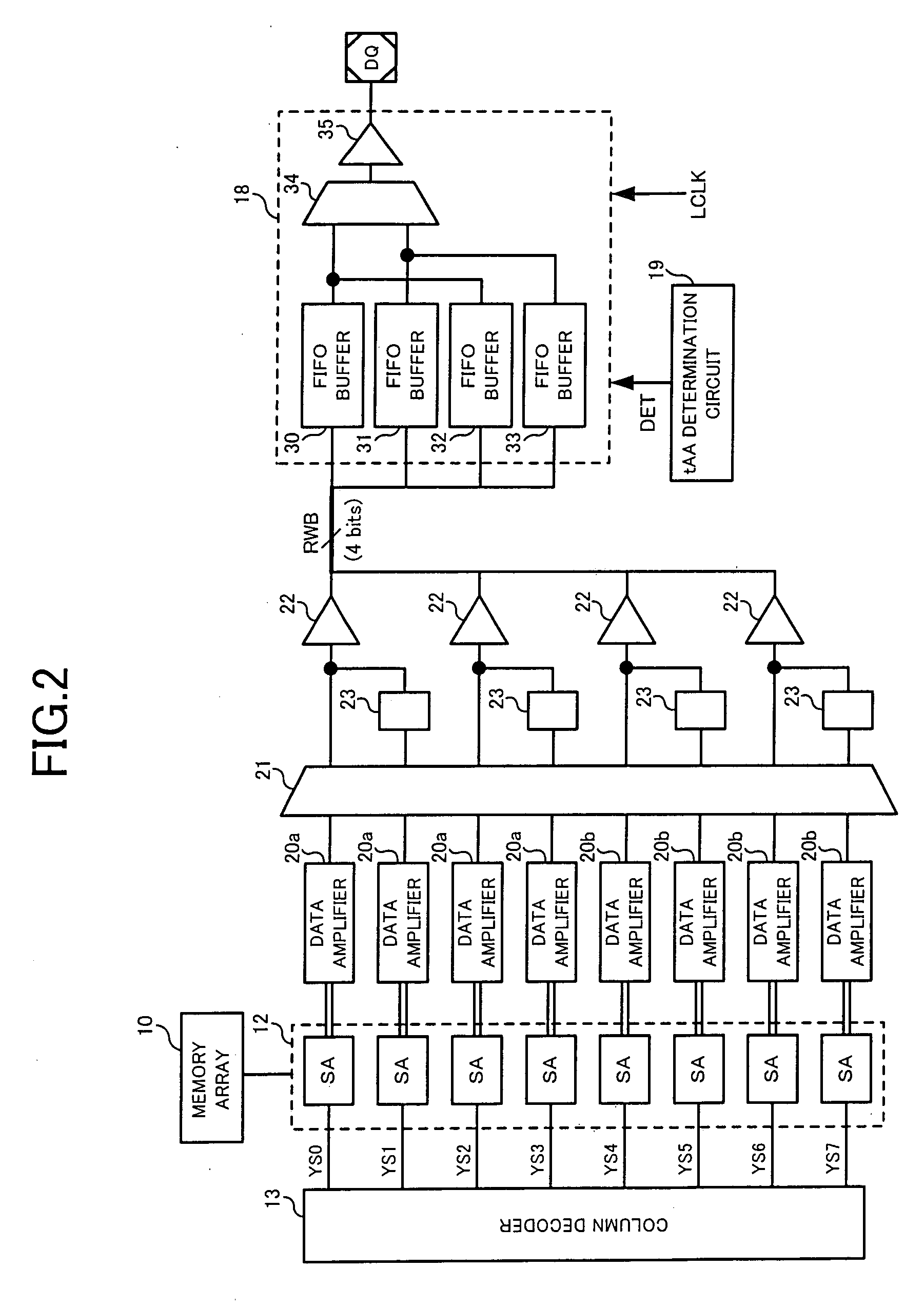
[0039]FIG. 1 is a block diagram showing a schematic configuration of the DRAM of this embodiment. The DRAM shown in FIG. 1 includes a memory array 10 for storing data; a row decoder 11, a sense amplifier unit 12 and a column decoder 13 which are provided on the periphery of the memory array 10; a row address buffer 14 and a column address buffer 15 which store addresses; a control circuit 16 for controlling operation of the entire DRAM; and an input buffer circuit 17 and an output buffer circuit 18 which transfer data input / output between the m...


PUM


Abstract

A semiconductor storage device comprising: a transfer control circuit for prefetching data of a predetermined number of bits stored in a memory array in response to a read command, and transferring L bits of the prefetched data in parallel to an internal bus in synchronization with an internal clock; and an output buffer circuit which includes L FIFO buffers each for latching each bit of the L bits input from the internal bus and extracts stored data from each of the L FIFO buffers in accordance with an input sequence in synchronization with an external clock so as to transfer the data serially to outside, wherein each of the L FIFO buffers includes an M-bit latch circuit and an N-bit latch circuit, and paths of the M-bit and N-bit latch circuits can be selectively switched.

Description

BACKGROUND OF THE INVENTION [0001] 1. Field of the Invention [0002] This invention relates to a semiconductor storage device which transfers data stored in a memory array to the outside in response to a read command, and particularly relates to a semiconductor storage device having a configuration for prefetching data of a predetermined number of bits to store in a output buffer circuit and transferring the data sequentially from the output buffer circuit to the outside. [0003] 2. Related Art [0004] In recent yeas, in order to control systems using semiconductor storage devices such as a DRAM (dynamic random access memories), there is a need for a technology for transferring data to the outside at high speed. For example, a DDR SDRAM (double-data-rate synchronous DRAMs) synchronizes with both rising and falling edges of an external clock to achieve higher-speed data transfer. In general, when data is read from the DRAM, access time from when a read command is issued until read data ...

Claims


Application Information

Patent Timeline
Patent Type & Authority Applications(United States)
IPC IPC(8): G11C16/04
CPCG11C7/1012G11C7/1039G11C7/1051G11C7/106G11C7/1066G11C7/1069G11C11/4096G11C2207/107
Inventor FUJISAWA, HIROKI
Owner MICRON TECH INC
Why Eureka
Try Eureka