Semiconductor devices having transistors with vertical channels and method of fabricating the same

a technology of semiconductor devices and transistors, which is applied in the direction of semiconductor devices, basic electric elements, electrical appliances, etc., can solve the problems of uneven width in the longitudinal direction of the bit line, excessive etching, and non-uniform resistance distribution of the bit line along the longitudinal direction

Inactive Publication Date: 2007-04-12
SAMSUNG ELECTRONICS CO LTD
View PDF4 Cites 153 Cited by
  • Summary
  • Abstract
  • Description
  • Claims
  • Application Information

AI Technical Summary

Benefits of technology

[0008] The present invention provides a semiconductor device configured to overcome the asymmetry limitation described above and configured to provide a buried bit line having a uniform resistance distribution along its length and a method of fabricating the same.

Problems solved by technology

The buried bit line formed as above has a problem in that its width is not uniform in the longitudinal direction of the bit line.
As a result, the resistance distribution of the bit line becomes non-uniform along its longitudinal direction.
Further, in order to perform the self-alignment etch process method to form a line-shaped bit line extending along a predetermined direction, it is restricted to design a plurality of active pillars such that a distance in the direction of the bit line and a distance in the direction perpendicular to the bit line based on each active pillar are different.
As such, when semiconductor devices are fabricated by the asymmetrical alignment design layout, an etch process of, for example, etching a conductive layer to form a cylindrical, ring-shaped, gate electrode formed to surround an outer circumference of the active pillar becomes unstable so that an excessive etch can occur in the relatively wider spaces while reduced etching, or lack of etching, can occur in relatively narrow areas, thereby reducing the process margin of the resulting devices.
Further, since the space that can be used to form a contact is limited, the process of forming the contact can be complicated.

Method used


Image

  • Semiconductor devices having transistors with vertical channels and method of fabricating the same
  • Semiconductor devices having transistors with vertical channels and method of fabricating the same
  • Semiconductor devices having transistors with vertical channels and method of fabricating the same

Examples


Embodiment Construction

[0045] The present invention will now be described more fully hereinafter with reference to the accompanying drawings, in which preferred embodiments of the invention are shown. This invention may, however, be embodied in many different forms and should not be construed as being limited to the embodiments set forth herein. Rather, these embodiments are provided so that this disclosure will be thorough and complete. Like numbers refer to like elements throughout the specification.

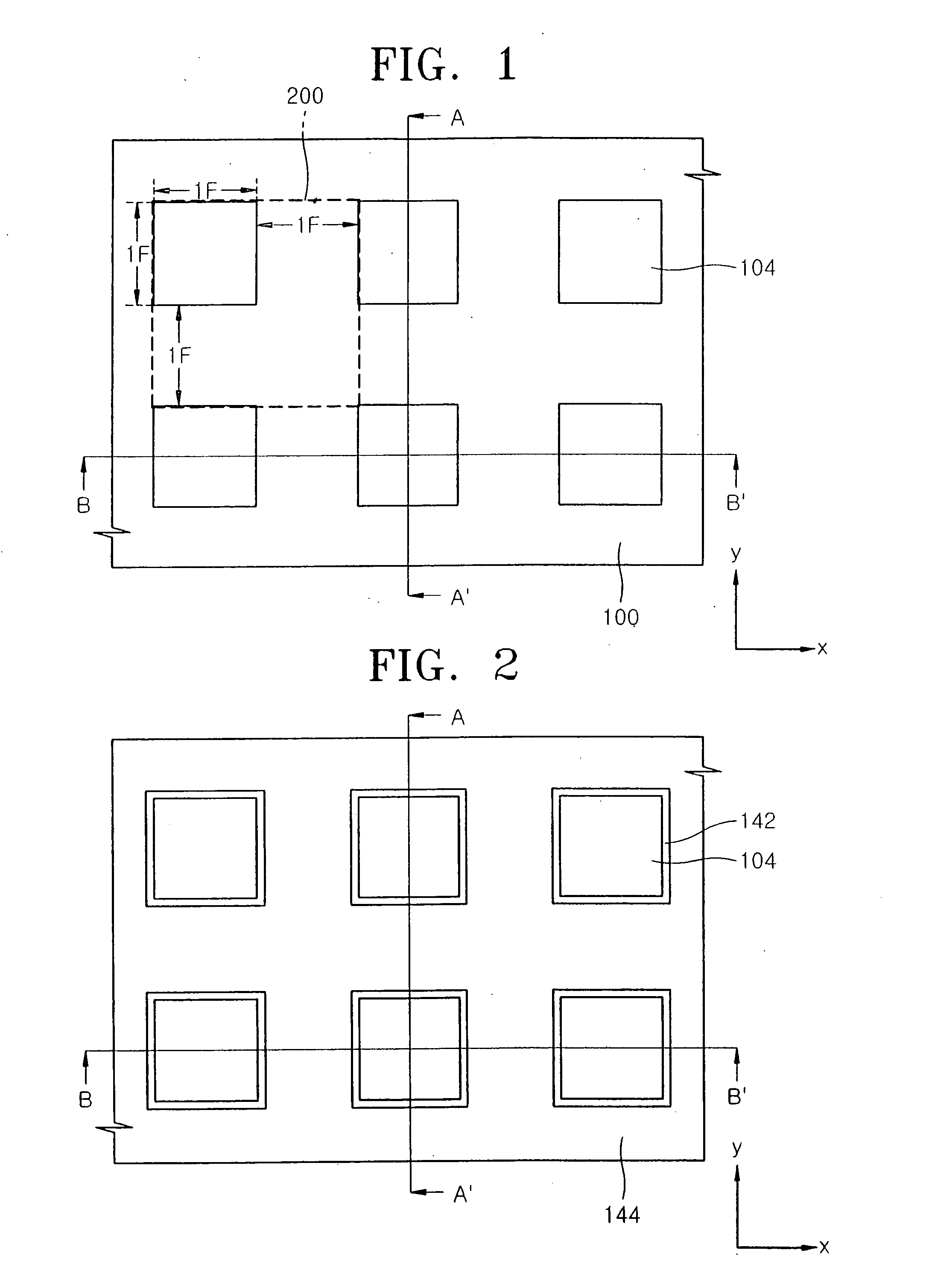
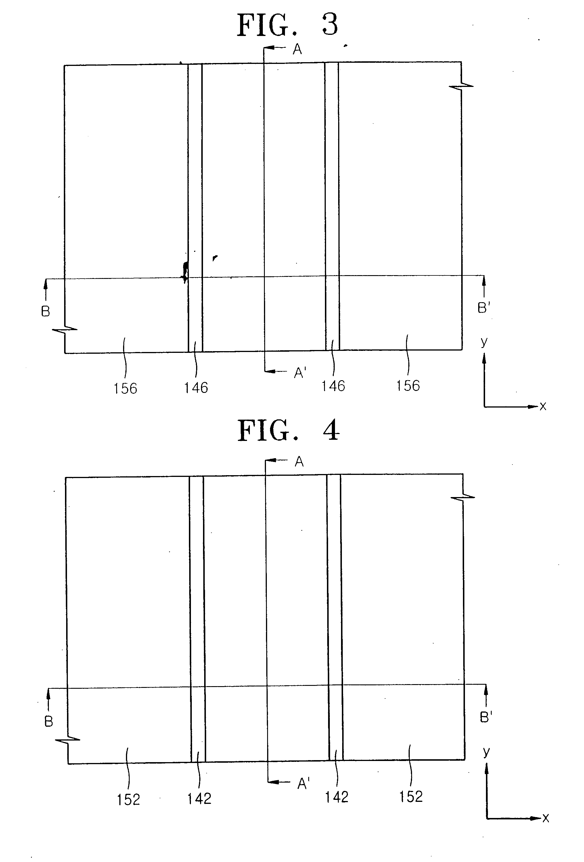
[0046]FIGS. 1 through 8 are schematic planar layouts illustrating a method of fabricating a semiconductor device in accordance with processing sequences according to an embodiment of the present invention. FIGS. 9A through 24A are sectional views taken along a line A-A′ of FIGS. 1 through 8 respectively, and FIGS. 9B through 24B are sectional views taken along a line B-B′ of FIGS. 1 through 8 respectively.

[0047] Referring to FIG. 1, FIG. 9A as a sectional view taken along a line A-A′ of FIG. 1, and FIG. 9B...


PUM


Abstract

In a semiconductor device and a method of fabricating the same, a vertical channel transistor has a cell occupation area of 4 F2. The semiconductor device comprises: a cell array region having a plurality of unit cells, each unit cell having a cell occupation area, repeatedly aligned along a first direction and along a second direction, the first and second directions being perpendicular to each other in a horizontal direction along a primary surface of a semiconductor substrate, wherein each unit cell has a uniform first pitch in the first direction and in the second direction; an active pillar vertically extending from an active region of each unit cell integrally with the semiconductor substrate in a vertical direction that is perpendicular with respect to the primary surface of the semiconductor substrate, wherein widths of at least a portion of the active pillar in the first direction and in the second direction are equal to a first width 1 F as a minimum feature size in the cell array region; a ring-shaped gate surrounding a sidewall of the active pillar; a channel region formed to extend along the active pillar in the vertical direction; a buried bit line formed below the active pillar in the semiconductor substrate; and a word line extending in the horizontal direction perpendicular to the buried bit line, and electrically connected to the ring-shaped gate, wherein a distance from the active pillar of any one unit cell of the plurality of unit cells to each of the active pillars of nearest neighboring unit cells in the first direction and the second direction is equal to the first width of the active pillar of one unit cell.

Description

CROSS-REFERENCE TO RELATED PATENT APPLICATION [0001] This application claims priority to Korean Patent Application No. 10-2005-0096169, filed on Oct. 12, 2005, in the Korean Intellectual Property Office, the contents of which are incorporated herein by reference in their entirety. BACKGROUND OF THE INVENTION [0002] 1. Field of the Invention [0003] The present invention relates to a semiconductor device having a vertical channel transistor and a method of fabricating the same, and more particularly, to a semiconductor device having a buried bit line formed below a vertical channel transistor, and a method of fabricating the same. [0004] 2. Description of the Related Art [0005] With the continued increase in the integration density of semiconductor memory devices, the planar area occupied by each unit cell becomes further reduced. In order to achieve a reduction of the unit cell area, there have been proposed various methods to form a transistor, a bit line, a word line, and a buried ...

Claims


Application Information

Patent Timeline
Patent Type & Authority Applications(United States)
IPC IPC(8): H01L21/336H01L29/76H01L29/94H01L31/00
CPCH01L27/10876H01L27/10885H01L29/66666H10B12/053H10B12/482H01L29/7827
Inventor KIM, BONG-SOOYOON, JAE-MANKIM, SEONG-GOOSEO, HYEOUNG-WONPARK, DONG-GUNLEE, KANG-YOON
Owner SAMSUNG ELECTRONICS CO LTD
Why Eureka
Try Eureka