Integrated circuit fabricating techniques employing sacrificial liners

a technology of integrated circuits and fabricating techniques, applied in the direction of basic electric elements, electrical equipment, semiconductor devices, etc., can solve the problems of difficulty or failure in meeting cd (critical design) parameters, residues are not soluble in resist solvents, and difficult to achiev

Inactive Publication Date: 2007-04-12
APPLIED MATERIALS INC
View PDF11 Cites 39 Cited by
  • Summary
  • Abstract
  • Description
  • Claims
  • Application Information

AI Technical Summary

Problems solved by technology

However, it is well known to persons of ordinary skill in the art that it is difficult to achieve this desirable result, since current and future IC fabricating methods and materials are likely to be affected by resist poisoning as will be described and illustrated in connection with IC structure 210 shown in FIG. 2.
Typically, these residues are not soluble in resist solvents that are utilized to remove exposed resist.
It is known that resist residues that are formed as a result of resist poisoning greatly interfere with anisotropically etching the underlying materials such as dielectric layer 218, thus resulting in difficulties or failure in meeting CD (critical design) parameters for etching a trench in a “via first” dual damascene fabricating procedure.
It is further kno

Method used


Image

  • Integrated circuit fabricating techniques employing sacrificial liners
  • Integrated circuit fabricating techniques employing sacrificial liners
  • Integrated circuit fabricating techniques employing sacrificial liners

Examples


Embodiment Construction

[0042] While describing the invention and its embodiments, certain technology will be utilized for the sake of clarity. It is intended that such terminology includes the recited embodiments as well as all equivalents.

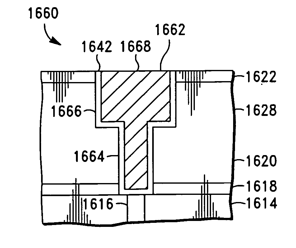
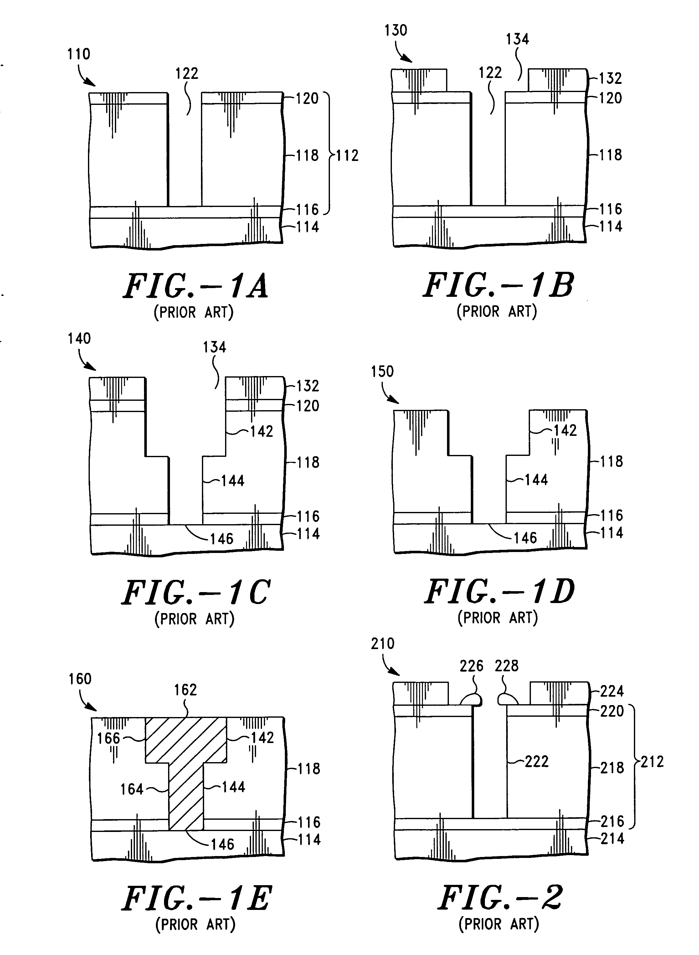
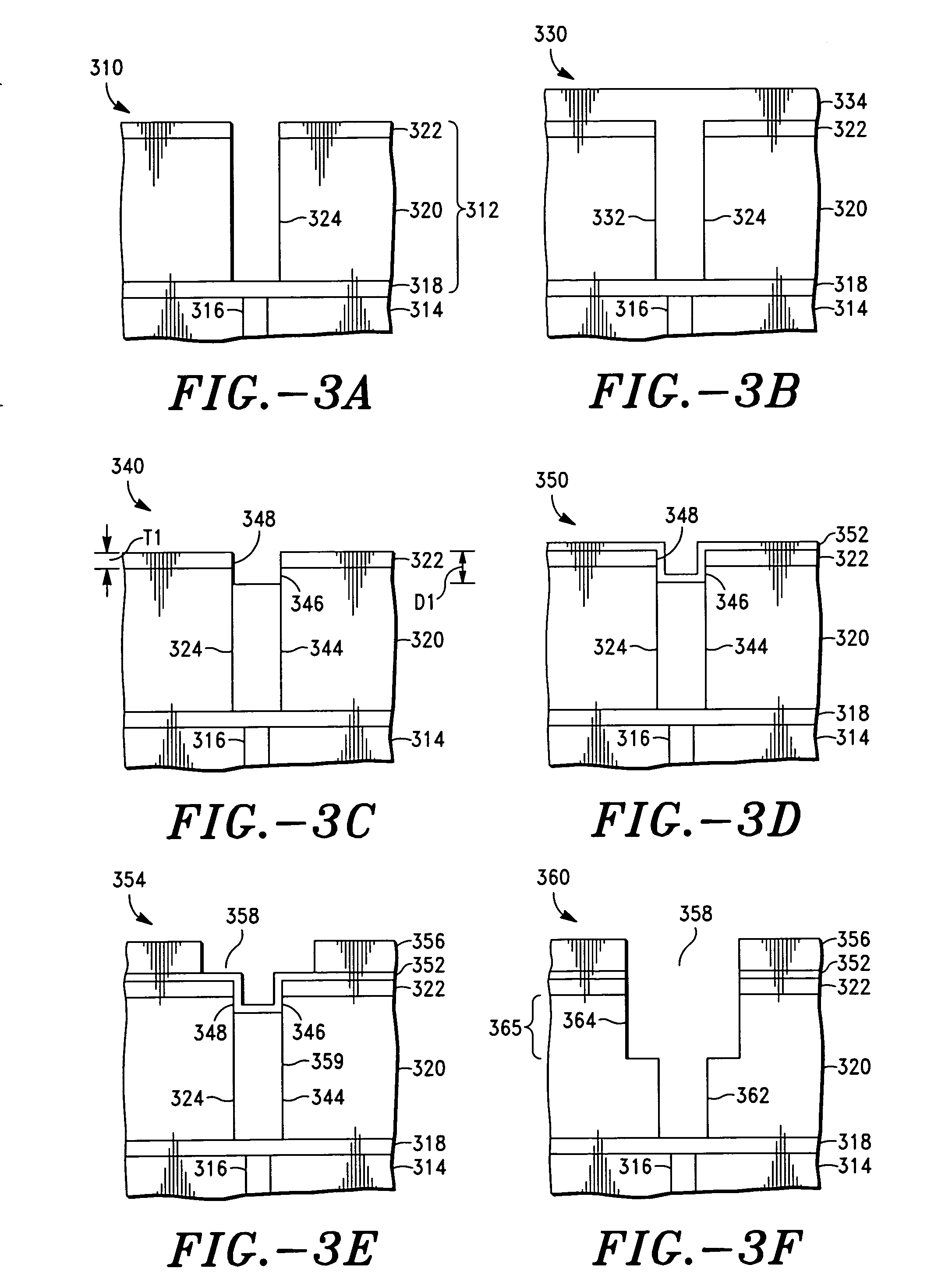
[0043] One embodiment, schematically illustrated in FIGS. 3A-31, shows a novel processing sequence, using a sacrificial fill and a sacrificial liner, for forming IC structures including IC structures having one or more dual damascene structures. The expression “integrated circuit structure” as defined herein, means completely formed integrated circuits and partially formed integrated circuits.

[0044]FIG. 3A shows an IC structure 310 including a dielectric stack 312 that is deposited on a substrate, such as a semiconductor substrate 314. The expression “semiconductor substrate” as defined herein, means structures and devices comprising typical IC elements, components, interconnects and semiconductor materials. Electrically conductive element 316, positioned in substrate...


PUM


Abstract

The present invention provides techniques for fabricating integrated circuit structures in semiconductor wafer fabrication. A via hole is prepared in a dielectric stack having a bottom via etch stop layer. The via hole is not extended through the via etch stop layer at this stage of the process. The via hole is partly filled with a sacrificial via fill such that a recess without sacrificial via fill is formed in the top portion of the via hole. A substantially conformal sacrificial layer is deposited on the top surface of the dielectric stack and in the recess. Then, a photoresist layer is deposited on the sacrificial fill. A trench etch mask overlaying the via hole, is developed in the photoresist layer. This mask is etched through the sacrificial layer that is formed on the top surface of the dielectric stack as well as through the sacrificial fill and sacrificial layer that is present in the via hole. Additionally, the mask is employed for etching a trench partly through the dielectric layer thereby forming a trench and an underlying via hole. The via hole is then extended through the via etch stop layer. Subsequently, the photoresist layer and the sacrificial layer are removed from the top surface of the dielectric stack resulting in a trench and underlying via hole that is suitable for fabricating a dual damascene structure. Alternatively, a recess can be formed by depositing a substantially conformal sacrificial layer on the top surface of the dielectric stack and in the via hole to form a lined via hole. The lined via hole is then partly filled with a sacrificial via fill such that a recess without sacrificial via fill is formed in the top portion of the lined via hole. Next, a photoresist layer is deposited in the recess and on the sacrificial liner that is deposited on the top surface of the dielectric stack.

Description

FIELD OF THE INVENTION [0001] The present invention relates to integrated circuit fabricating techniques wherein sacrificial liners and sacrificial fills are employed to substantially reduce or prevent photoresist poisoning. BACKGROUND OF THE INVENTION [0002] A semiconductor device such as an IC (integrated circuit) generally has electronic circuit elements such as transistors, diodes and resistors fabricated integrally on a single body of semiconductor material. The various circuit elements are connected through conductive connectors to form a complete circuit which can contain millions of individual circuit elements. Advances in semiconductor materials and processing techniques have resulted in reducing the overall size of the IC circuit elements while increasing their number on a single body. Additional miniaturization is highly desirable for improved IC performance and cost reduction. Interconnects provide the electrical connections between the various electronic elements of an ...

Claims


Application Information

Patent Timeline
IPC IPC(8): H01L21/4763H01L29/76H01L29/94H01L31/00
CPCH01L21/76808H01L21/76877
Inventor NAIK, MEHULGANDIKOTA, SRINIVASDIXIT, GIRISHYOST, DENNIS
Owner APPLIED MATERIALS INC
Why Eureka
Try Eureka