
Charged particle beam device with DF-STEM image valuation method

a charge particle and beam device technology, applied in the field of charge particle beam devices, can solve the problem of not always obtaining images which intensely reflect the atomic number contras

Inactive Publication Date: 2007-04-19
HITACHI HIGH-TECH CORP
View PDF3 Cites 14 Cited by
  • Summary
  • Abstract
  • Description
  • Claims
  • Application Information

AI Technical Summary

Benefits of technology

[0011] According to the present invention, it is possible to obtain information by which it is judged whether or not the dark-field image has an appropriate atomic number contrast.

Problems solved by technology

Therefore, even when the same sample is observed, the image which intensely reflects the atomic number contrast is not constantly obtained.

Method used


Image

  • Charged particle beam device with DF-STEM image valuation method
  • Charged particle beam device with DF-STEM image valuation method
  • Charged particle beam device with DF-STEM image valuation method

Examples


embodiment 2

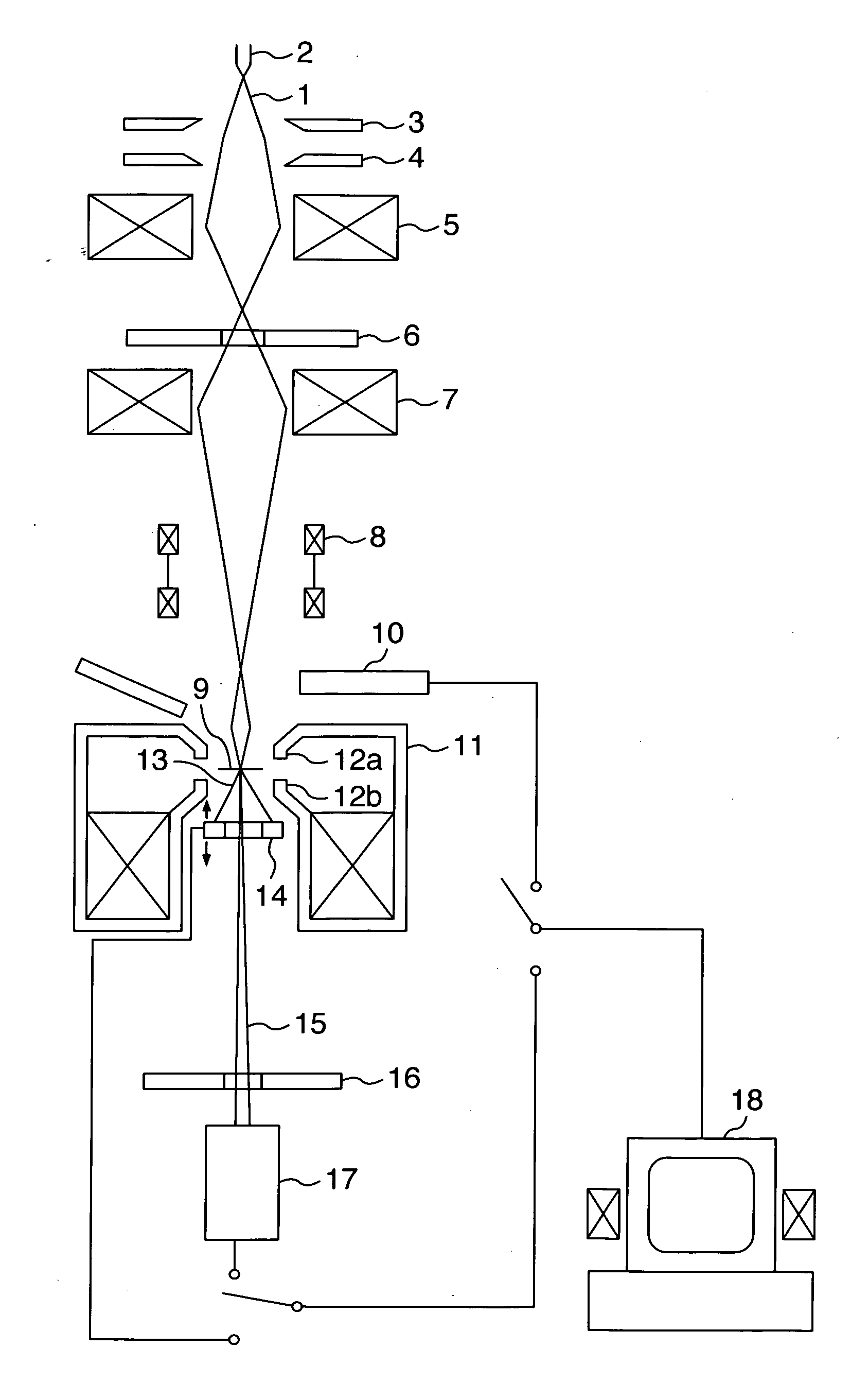
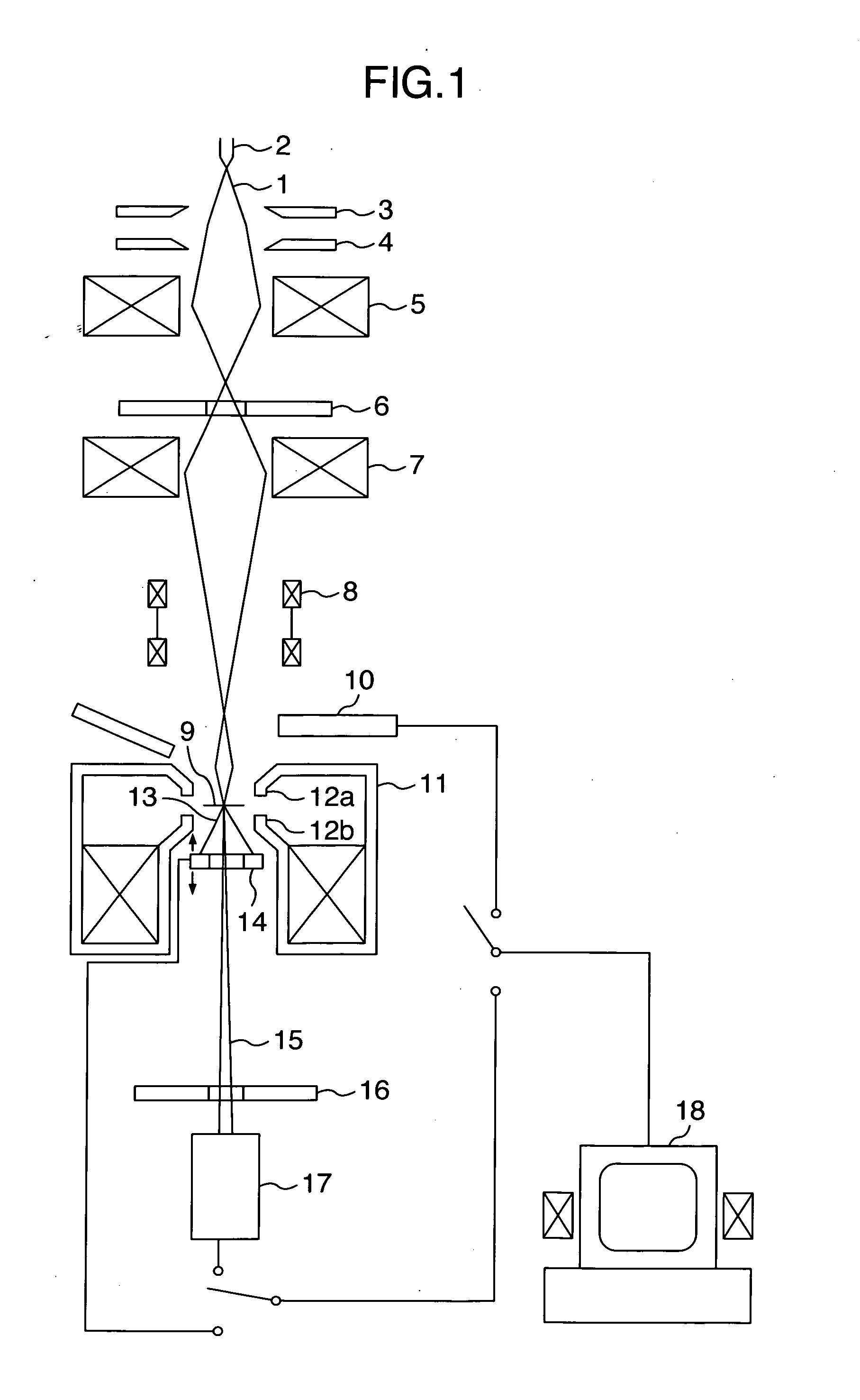
[0060] There will be described hereinafter a device capable of determining observation conditions based on a scattering angle region predicting simulation of a transmission electron with reference to the drawings.

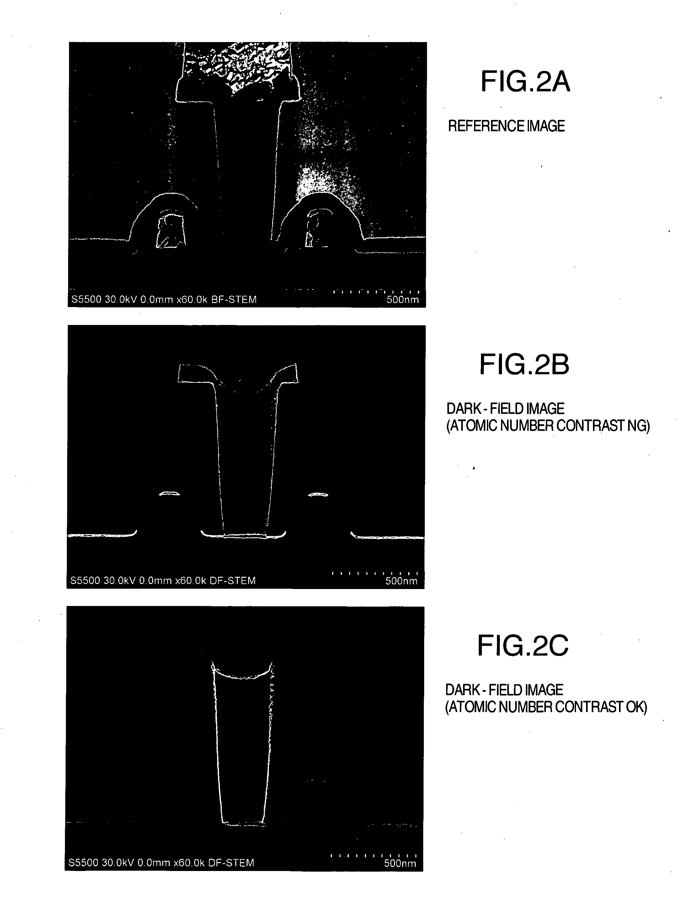
[0061] In Embodiment 1, it has mainly been described that a dark-field image for valuation is acquired beforehand and compared with a bright-field image to judge whether or not an image based on the resultant dark-field signal has an appropriate contrast. To acquire this dark-field image for the valuation, it is necessary to grasp beforehand a knowledge concerning a transmission electron image or approximately a principle of a device optical system.

[0062] Moreover, when conditions for acquiring the dark-field image for the valuation are different from ideal conditions, the number of images until optimum observing conditions are reached is large. Therefore, it is necessary to efficiently reach the optimum observing conditions in consideration of a risk of a beam damage or ...

case 1

(Case 1) There is detected a scattering region having a remarkably small angle as compared with the optimum scattering detection angle region.

case 2

(Case 2) There is detected a scattering region having a remarkably large angle as compared with the optimum scattering detection angle region.

[0100] In Case 1, a part or all of the resultant dark-field image indicates a contrast equal to that of the bright-field image. Therefore, there may be imparted a mechanism to detect whether or not the image includes information (contrast) of the bright-field image, and optical conditions may be adjusted so as to detect a larger scattering angle region if any. Moreover, there may be set beforehand a degree of shift of the detection region to a large angle side in a case where bright-field information is detected, and the optical conditions may automatically be adjusted. As the mechanism to detect the information of the bright-field image, line scanning of the valuation image (dark-field image) and the reference image (bright-field image) is performed. When both waveform patterns agree with each other or are similar to each other, it can be jud...


PUM


Abstract

There is disclosed a charged particle beam device which judges whether or not an image based on a dark-field signal has an appropriate atomic number contrast. Input reference information, a bright-field image or a back-scattered electron image is compared with a dark-field image, and it is judged whether or not a correlation value between them or the dark-field image has a predetermined contrast. According to such a constitution, it is possible to obtain information by which it is judged whether or not the dark-field image has an appropriate atomic number contrast.

Description

BACKGROUND OF THE INVENTION [0001] 1. Field of the Invention [0002] The present invention relates to a charged particle beam device, more particularly to a charged particle beam device preferable for detecting signal particles scattered in a sample and transmitted through the sample distinctively from signal particles transmitted through the sample without being scattered to obtain a sample image due to an atomic number difference from the signal particles scattered in the sample and transmitted through the sample. [0003] 2. Description of the Related Art [0004] In a charged particle beam device represented by a scanning electron microscope, a charged particle beam thinly converged is scanned on a sample to obtain desired information (e.g., a sample image) from the sample. Much of such charged particle beam devices is used in valuation of a semiconductor device and analysis of defects. Since miniaturizing and multilayer-structuring of the semiconductor device have yearly advanced, a...

Claims


Application Information

Patent Timeline
IPC IPC(8): G21K7/00
CPCH01J37/265H01J2237/221
Inventor ARAKI, MINEWATANABE, SHUNYAKAMIYA, CHISATOSATO, MITSUGUTAKANE, ATSUSHIMORIKAWA, AKINARIMIYAKI, ATSUSHIISHITANI, TORU
Owner HITACHI HIGH-TECH CORP
Learn More