Method for preparing a phase-shifting mask and method for preparing a semiconductor device using the phase-shifting mask

a technology of phase shift mask and semiconductor device, which is applied in the field of preparation of phase shift mask and the preparation of semiconductor device using the phase shift mask, can solve the problems of mask inspection and phase error, increase the difficulty of alignment, and restrict the mask throughput, so as to eliminate the problem of phase error and increase the mask throughput

Inactive Publication Date: 2007-04-19
PROMOS TECH INC
View PDF10 Cites 5 Cited by
  • Summary
  • Abstract
  • Description
  • Claims
  • Application Information

AI Technical Summary

Benefits of technology

[0010] The primary objective of the present invention is to provide a method for preparing a phase-shifting mask having phase-shifting patterns made of polymer material and a method for preparing a semiconductor device using the phase-shifting mask, which can increase mask throughput, eliminate the phase error problem and mask inspection issue, and solve the imaging problem of the OAI technique in cases where masks have equal line width and space width.

Problems solved by technology

The prior art needs to perform the lithographic process twice, which increases the alignment difficulty and restricts the mask throughput.
The prior art prepares the phase-shifting pattern by etching the quartz substrate, which generates issues of mask inspection and phase error.

Method used


Image

  • Method for preparing a phase-shifting mask and method for preparing a semiconductor device using the phase-shifting mask
  • Method for preparing a phase-shifting mask and method for preparing a semiconductor device using the phase-shifting mask
  • Method for preparing a phase-shifting mask and method for preparing a semiconductor device using the phase-shifting mask

Examples


Embodiment Construction

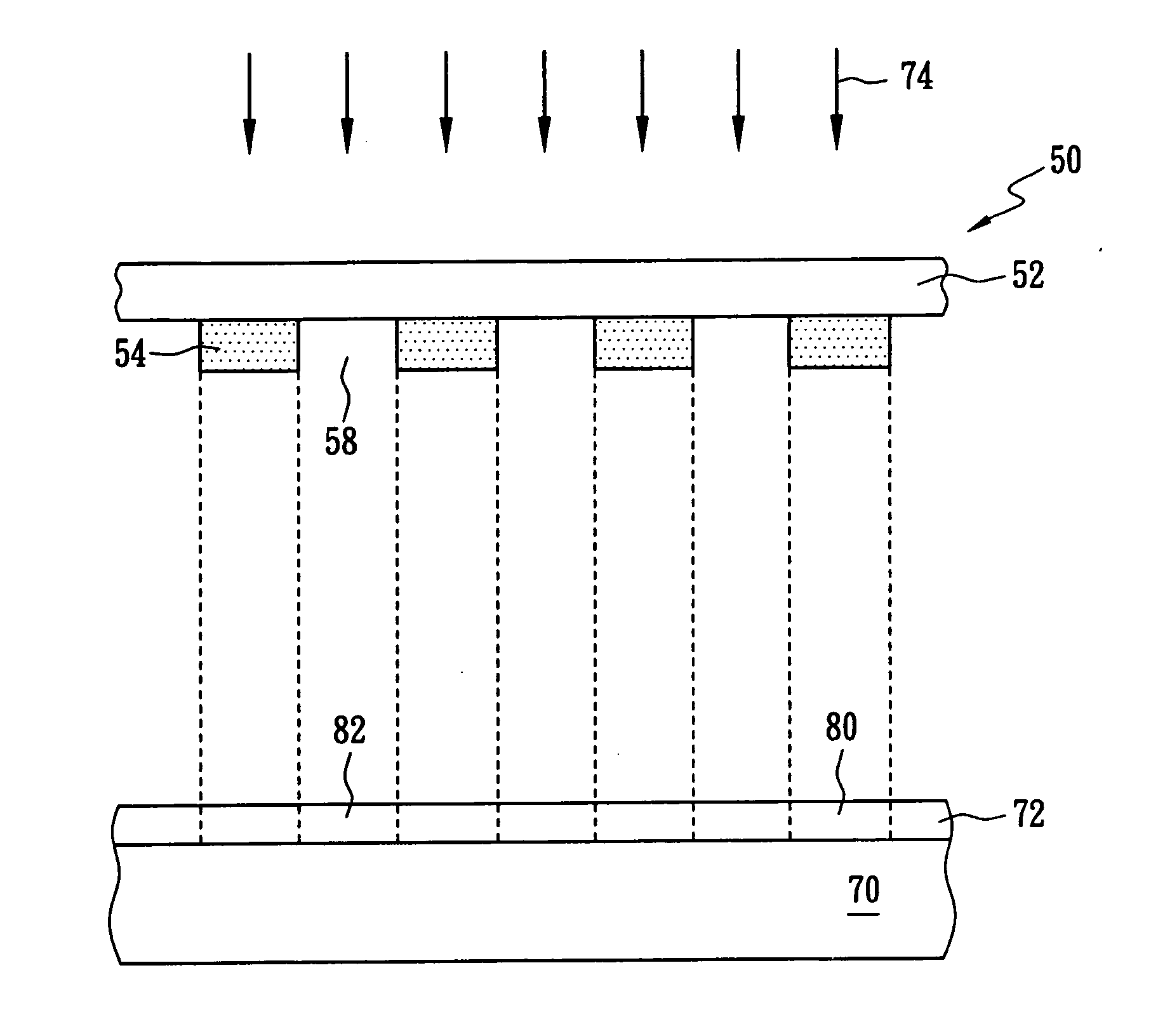
[0025]FIG. 7 to FIG. 9 illustrate a method for preparing a chromeless phase-shifting mask 50 according to one embodiment of the present invention. A spin-coating process is performed to form a polymer layer 62 on a substrate 52, and energy is then selectively transferred to a portion of the polymer layer 62 in a plurality of predetermined regions 66 arranged in an array manner, such as irradiating an electron beam 64 to the predetermined region 66, to change the chemical properties of the polymer layer 62 in the predetermined region 66, i.e., to change the molecular structure of the polymer layer 62 in the predetermined regions 66. Particularly, the electron beam 64 provides energy to activate the polymer in the predetermined region 66 to change its molecular structure such as forming cross-linking.

[0026] Referring to FIG. 8, a developing process is performed to remove a portion of the polymer layer 62 not irradiated by the electron beam 64, i.e., the polymer layer 62 outside the p...


PUM

PropertyMeasurementUnit
wavelengthaaaaaaaaaa
phase-shifting angleaaaaaaaaaa

Abstract

A phase-shifting mask comprises a substrate and a plurality of phase-shifting patterns made of polymer material and positioned on the substrate in an array manner. Preferably, the space between phase-shifting patterns is smaller than the width of the phase-shifting pattern along a first direction, and the space between two line-shaped patterns consisting of phase-shifting patterns is substantially equal to the width of the line-shaped pattern along a second direction perpendicular to the first direction. The present method for preparing the phase-shifting mask comprises steps of forming a polymer layer on a substrate, changing the molecular structure the polymer layer in a plurality of predetermined regions, and removing a portion of the polymer layer outside these predetermined regions. The polymer layer can be made of hydrogen silsesquioxane, methylsilsesquioxane or hybrid organic siloxane polymer.

Description

BACKGROUND OF THE INVENTION [0001] (A) Field of the Invention [0002] The present invention relates to a method for preparing a phase-shifting mask and a method for preparing a semiconductor device using the phase-shifting mask, and more particularly, to a method for preparing a phase-shifting mask having phase-shifting patterns made of polymer material and a method for preparing a semiconductor device using the phase-shifting mask. [0003] (B) Description of the Related Art [0004] As the integration density of semiconductor devices increases, the lithographic process needs a higher resolution to meet the precision requirement of the semiconductor device. One method to increase resolution is to use a light source with a shorter wavelength as the exposure light. For example, the krypton fluoride (KrF) laser is used to provide deep UV light with a wavelength of 248 nanometers, and the argon fluoride (ArF) laser is used to provide deep UV light with a wavelength of 193 nanometers. Anothe...

Claims


Application Information

Patent Timeline
Patent Type & Authority Applications(United States)
IPC IPC(8): G03C5/00G03F9/00G03F1/00
CPCG03F1/34
Inventor LAI, YEE KAI
Owner PROMOS TECH INC
Why Eureka
Try Eureka