Method for manufacturing semiconductor device

a manufacturing method and semiconductor technology, applied in semiconductor/solid-state device manufacturing, basic electric elements, electric devices, etc., can solve the problems of reducing the height dimension of the element isolation film from the surface of the substrate, increasing the amount of etched silicon nitride film, and difficulty in adjusting the height dimension of the element isolation film from the substrate surface, so as to achieve the desired thickness, less variation in the thickness of the silicon nitride film, and less height dimension variation

Inactive Publication Date: 2007-04-19
RENESAS ELECTRONICS CORP
View PDF5 Cites 9 Cited by
  • Summary
  • Abstract
  • Description
  • Claims
  • Application Information

AI Technical Summary

Benefits of technology

[0011] Since the protective film covering the silicon nitride film is utilized as a mask during the etch process for forming the trenched portion in the present invention, the silicon nitride film is protected by the protective film during the etch process for forming the trenched portion. Therefore, the silicon nitride film is less to be affected by the etch process for forming the trenched portion. Therefore, in the present invention, a silicon nitride film having a desired thickness can be assured, even if the etch process for forming the trenched portion is conducted. Then the protective film is removed, and thereafter, the element isolation film is deposited, and then the element isolation film formed on the silicon nitride film is removed via the polishing process, so that the silicon nitride film, which has been least to be affected by the etch process for forming the trenched portion and has a predetermined thickness, can be employed as a stop film utilized in the polishing process. Therefore, according to the present invention, an element isolation film having a desired height dimension can be formed. Further, since the silicon nitride film is less to be affected by the etch process for forming the trenched portion in the present invention, a variation in the thickness of the silicon nitride film is less to be caused. Therefore, a variation in the height dimension of the element isolation film from the surface of the substrate can be inhibited.
[0012] According to the present invention, a semiconductor device comprising an element isolation film, which exhibits less variations in the height dimension from the surface of the substrate and has a desired height dimension from the surface of the substrate, is provided.

Problems solved by technology

Therefore, a decrease in the amount of the precipitates causes an increase in an amount of the etched silicon nitride film.
When the silicon nitride film that is thinner in thickness is employed as a stop film for a CMP process, the height dimension of the element isolation film from the surface of the substrate is reduced, so that an adjustment of the height dimension of the element isolation film from the surface of the substrate would be difficult.
Further, an increase in the amount of the etched silicon nitride film leads to an uneven etching of the silicon nitride film, so that it is difficult to obtain an element isolation film having an even and uniform height dimension.
But in such case, a variation in the height dimension of the element isolation film causes a difficulty in providing a well which has a desired depth.

Method used


Image

  • Method for manufacturing semiconductor device
  • Method for manufacturing semiconductor device
  • Method for manufacturing semiconductor device

Examples


example

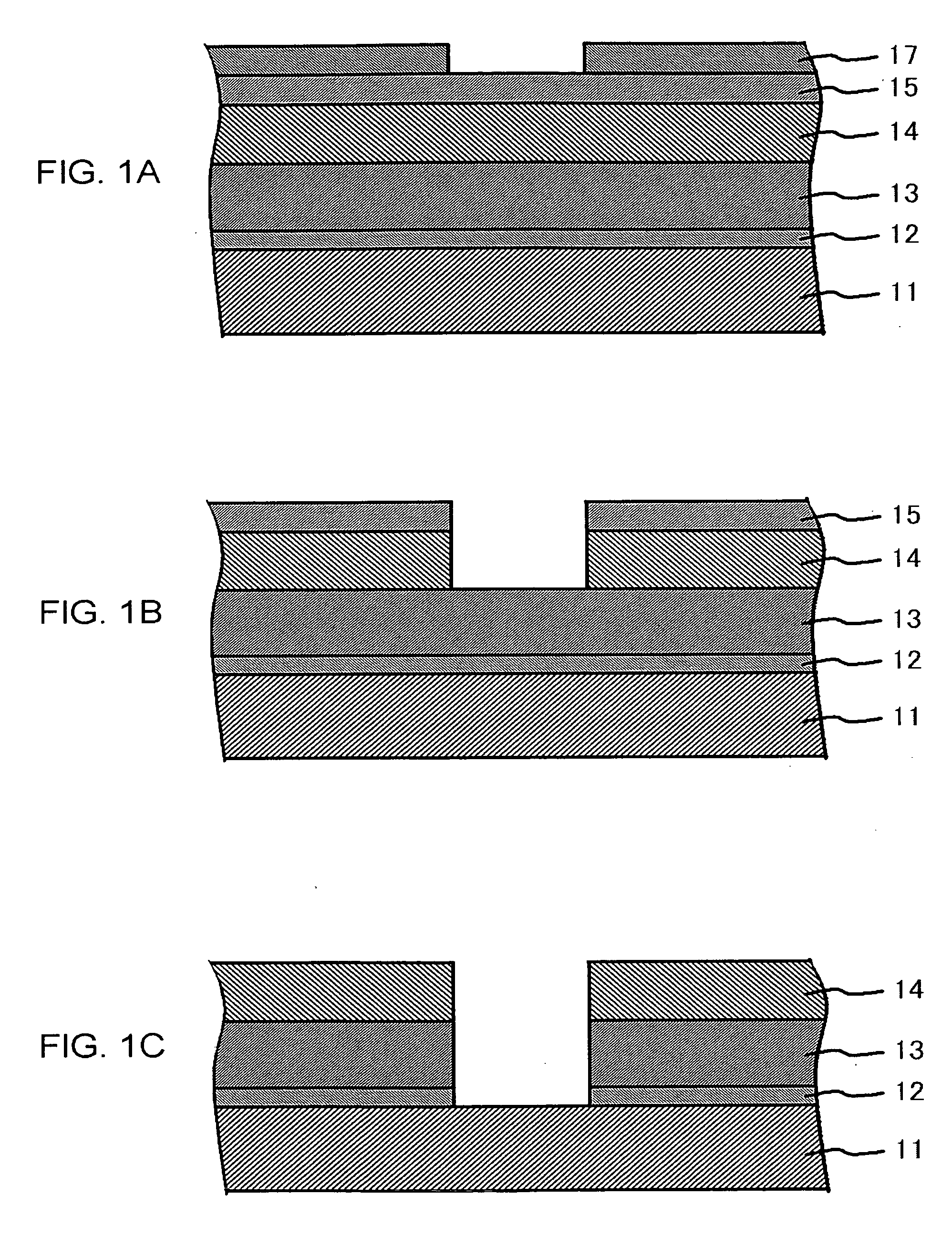
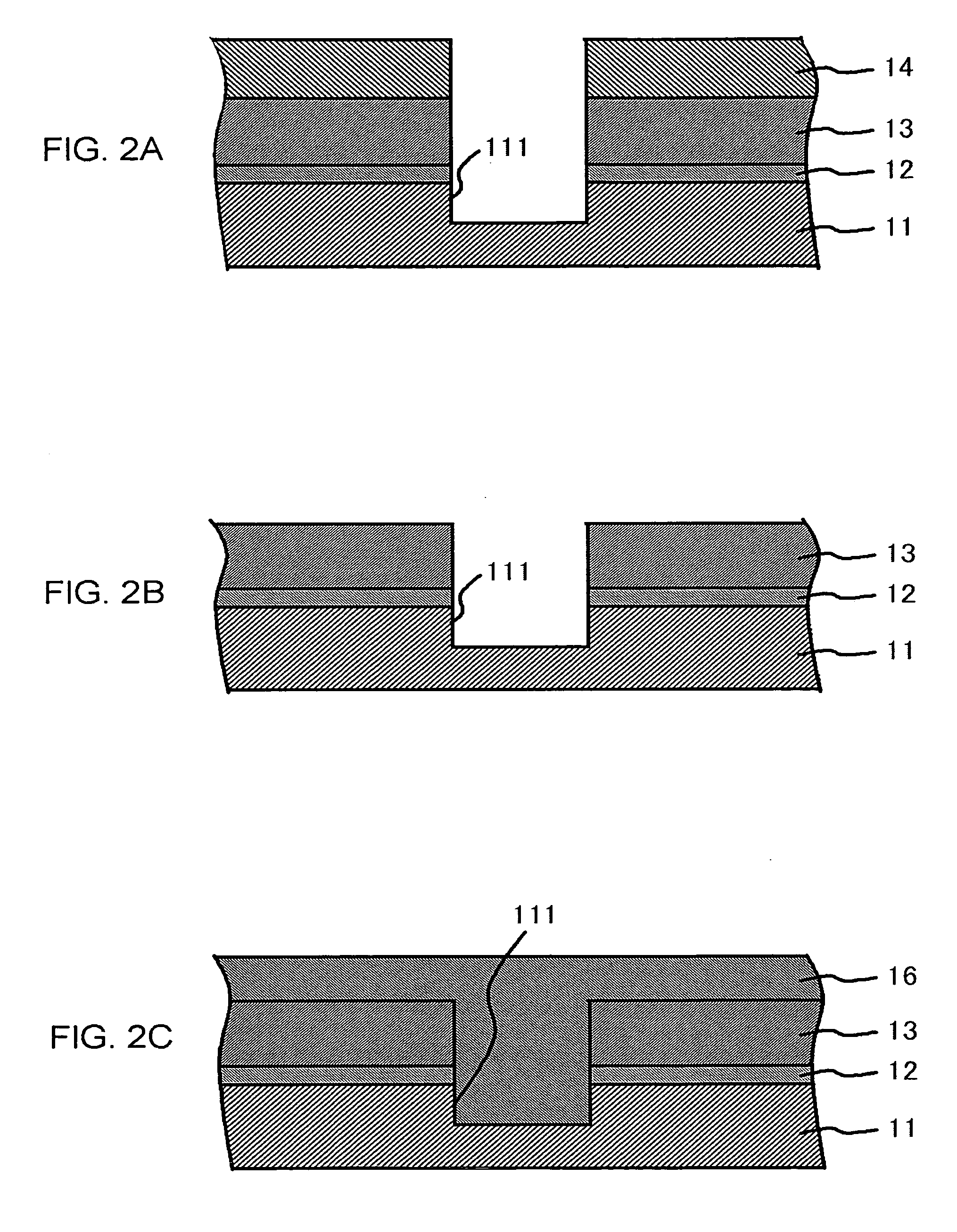
[0040] An example of the present invention will be described. A formation of an element isolation film was conducted in a process similar to that described in the above embodiment. Similarly as in the above-described embodiment, a silicon oxide film (thickness: 10 nm) was formed on a silicon substrate, and a silicon nitride film (thickness: 120 nm), an amorphous carbon film (thickness: 120 nm) and an inorganic film (SiOC film, thickness: 30 nm) were deposited on the silicon oxide film.

[0041] Next, a mask having a predetermined pattern was formed on the inorganic film, and then the inorganic film was dry etched with SF6 gas at a pressure of 5 mTorr. Further, a gaseous mixture of O2 gas and HBr gas was employed to generate a plasma, and then the amorphous carbon film was dry etched. In this case, the mask on inorganic film was removed by the dry etch process. On the contrary, substantially no inorganic film itself was removed. A selectivity presented by (etch rate for amorphous carbo...


PUM

PropertyMeasurementUnit
thicknessaaaaaaaaaa
thicknessaaaaaaaaaa
thicknessaaaaaaaaaa

Abstract

A semiconductor device includes an element isolation film, which exhibits less variations in the height dimension from the surface of the substrate and has a desired height dimension from the surface of the substrate. A process for manufacturing a semiconductor device includes: providing a predetermined pattern of a silicon nitride film and a protective film which covers the silicon nitride film, on a semiconductor substrate; selectively etching the semiconductor substrate using the protective film as a mask to form a trenched portion; removing the protective film to expose the silicon nitride film; depositing an element isolation film, so as to fill the trenched portion therewith and cover the silicon nitride film; removing the element isolation film formed on the silicon nitride film by polishing thereof until the silicon nitride film is exposed; and removing the silicon nitride film.

Description

[0001] This application is based on Japanese patent application No. 2005-302,056, the content of which is incorporated hereinto by reference. BACKGROUND [0002] 1. Field of the Invention [0003] The present invention relates to a method for manufacturing a semiconductor device, and particularly relates to a technology for forming an element isolation film. [0004] 2. Related Art [0005] Conventionally, a region for forming a transistor and an element isolation region are created on a semiconductor substrate. The element isolation region is formed as described below, for example. As shown in FIG. 4A, a thin film 901 is provided so as to cover a region for forming the transistor on a semiconductor substrate 900, and further, as shown in FIG. 4B, a silicon nitride film 902 is provided on the thin film 901. The thin film 901 is one that is harder than a silicon nitride film 902. Thereafter, as shown in FIG. 4C, the semiconductor substrate 900 is etched through a mask of the silicon nitride ...

Claims


Application Information

Patent Timeline
Patent Type & Authority Applications(United States)
IPC IPC(8): H01L21/76
CPCH01L21/76224
Inventor MITSUIKI, AKIRANAKAYAMA, TOMOOFUJITA, OSAMU
Owner RENESAS ELECTRONICS CORP
Why Eureka
Try Eureka