Wafer producing method and processing feed direction detecting method

a technology of detecting method and producing method, which is applied in the direction of manufacturing tools, crystal growth process, after-treatment details, etc., can solve the problems of high hardness of single crystal sic ingots, poor productivity of wafer production, and obstacles to the efficient generation of wafers. achieve the effect of improving productivity

Active Publication Date: 2019-09-10
DISCO CORP
View PDF83 Cites 8 Cited by
  • Summary
  • Abstract
  • Description
  • Claims
  • Application Information

AI Technical Summary

Benefits of technology

[0005]It is an object of the present invention to provide a wafer producing method that can improve productivity.
[0006]Another object of the present invention is to provide a processing feed direction detecting method making it possible to carry out the wafer producing method that can improve productivity.
[0009]The wafer producing method according to the present invention is capable of producing a wafer having a desired thickness by peeling off a portion of the single-crystal SiC ingot from the peeling plane serving as a boundary plane. Wafers can efficiently be produced from the single-crystal SiC ingot. The amount of wafer material that has to be thrown away is reduced. Wafers can be produced from the single-crystal SiC ingot with improved productivity.
[0010]The processing feed direction detecting method according to the present invention determines a direction in which the straight sampled reduced strength area where the measured number of nodes is zero extends as a processing feed direction. Therefore, the processing feed direction is made perpendicular to the direction in which the c-axis is inclined. Consequently, a peeling plane of good quality can reliably be formed for the generation of wafers from the single-crystal SiC ingot.

Problems solved by technology

One problem with slicing an ingot into a wafer with a wire saw and polishing the upper and lower surfaces of the wafer is that it is uneconomical because most (70% through 80%) of the ingot has to be thrown away.
In particular, single-crystal SiC ingots have high hardness and have a productivity problem because slicing them with a wire saw is a difficult task to perform and takes a considerable period of time, are highly costly each, and present an obstacle to the efficient generation of wafers.
However, producing wafers from an SiC ingot suffers poor productivity as a number of adjacent modified layers need to be formed in the SiC ingot.

Method used


Image

  • Wafer producing method and processing feed direction detecting method
  • Wafer producing method and processing feed direction detecting method
  • Wafer producing method and processing feed direction detecting method

Examples


Embodiment Construction

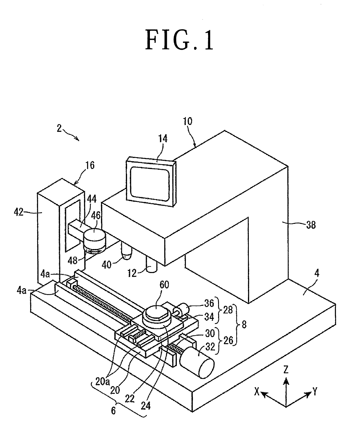
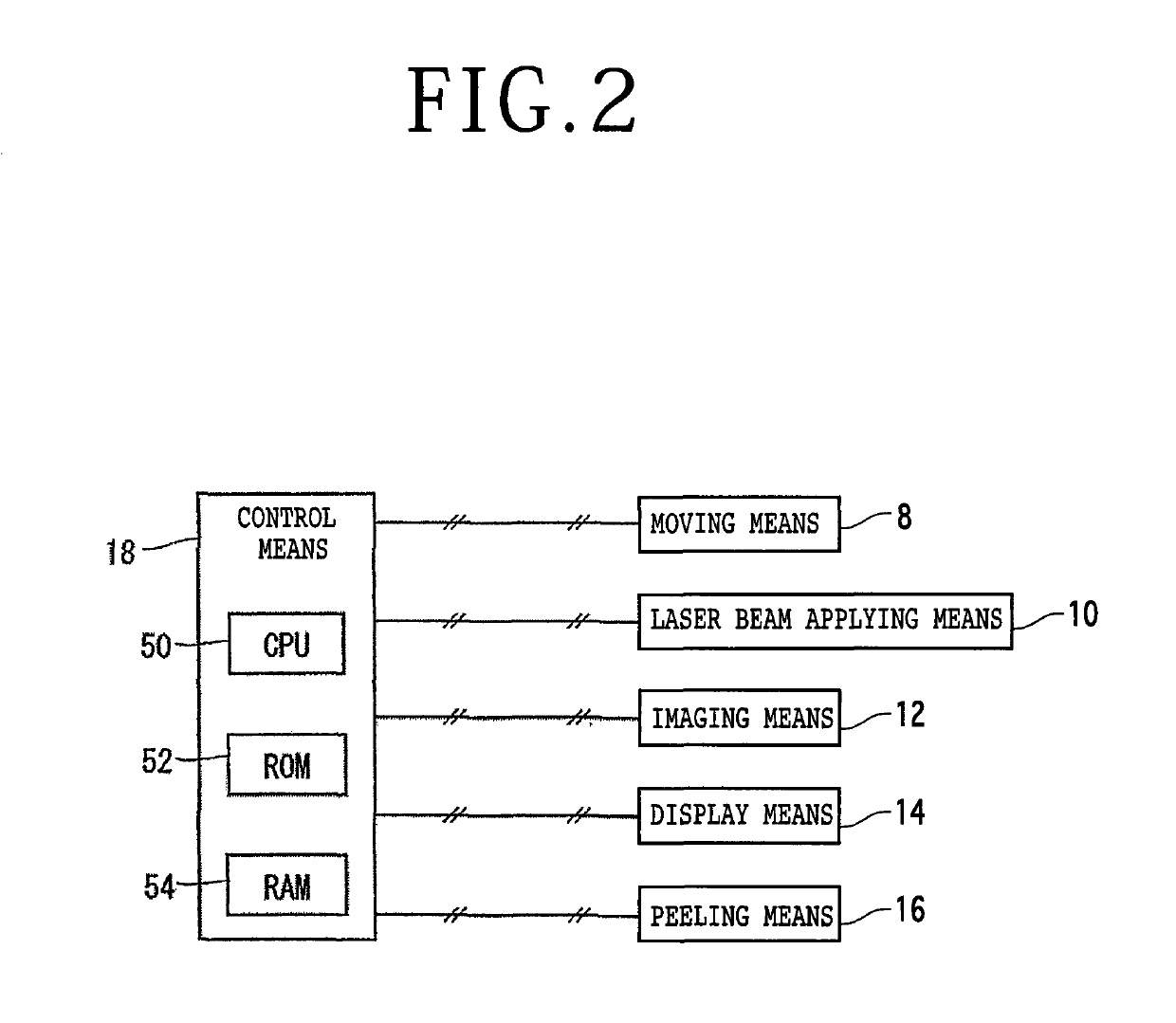
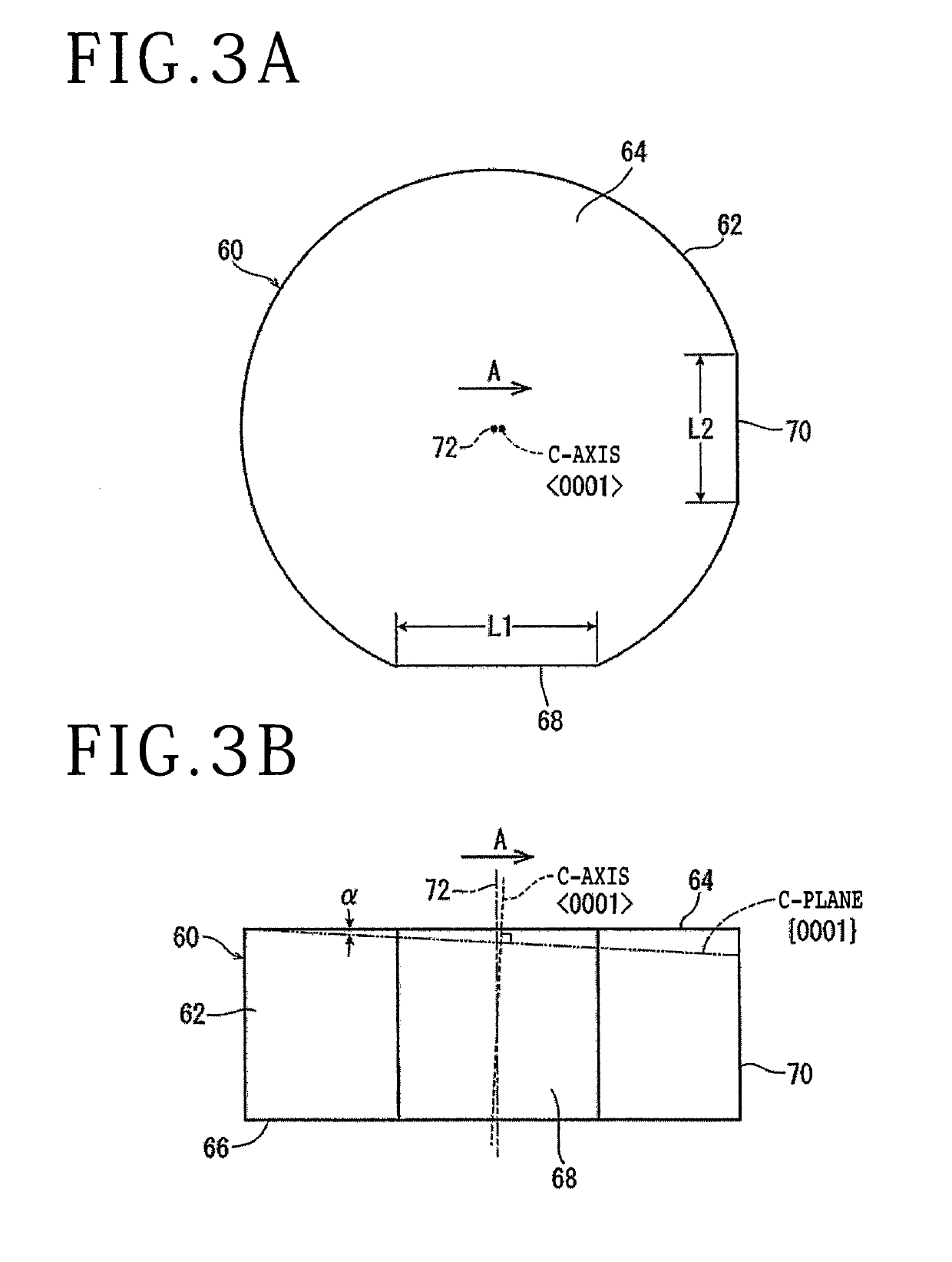
[0024]A wafer producing method and a processing feed direction detecting method according to a preferred embodiment of the present invention will be described below with reference to the drawings. First, a laser processing apparatus 2 shown in FIGS. 1 and 2 and a hexagonal single-crystal SiC ingot 60 shown in FIGS. 3A and 3B, which are to be used in the methods, will be described below. As shown in FIG. 1, a laser processing apparatus 2 has a base table 4, holding means 6 for holding a workpiece, moving means 8 for moving the holding means 6, laser beam applying means 10, imaging means 12, display means 14, peeling means 16, and control means 18.

[0025]The holding means 6 includes a rectangular X-direction movable plate 20 mounted on the base table 4 for movement in X directions, a rectangular Y-direction movable plate 22 mounted on the X-direction movable plate 20 for movement in Y directions, and a cylindrical chuck table 24 rotatably mounted on an upper surface of the Y-direction ...


PUM

PropertyMeasurementUnit
lengthaaaaaaaaaa
length Lcaaaaaaaaaa
length Lcaaaaaaaaaa

Abstract

A wafer is produced from an ingot by confirming whether or not an inclined c-axis of the ingot and a second orientation flat of the ingot are perpendicular to each other, and detecting a processing feed direction perpendicular to the direction in which the c-axis is inclined. The method includes performing sampling irradiation of the ingot with a laser beam, along a direction parallel to the second orientation flat and a plurality of directions inclined clockwise and counterclockwise by respective predetermined angles from the second orientation flat, thereby forming a plurality of sampled reduced strength areas in the ingot; measuring the number of nodes which exist per unit length on each of the sampled reduced strength areas, and determining a direction in which the sampled reduced strength area where the measured number of nodes is zero extends as a processing feed direction.

Description

BACKGROUND OF THE INVENTIONField of the Invention[0001]The present invention relates to a wafer producing method of producing a wafer from a single-crystal SiC ingot and a processing feed direction detecting method of detecting a processing feed direction perpendicular to the direction in which a c-axis is inclined at the time a wafer is produced from a single-crystal SiC ingot.Description of the Related Art[0002]Devices such as integrated circuits (ICs), large scale integration (LSI) circuits, light emitting diodes (LEDs), etc. are produced by depositing functional layers on the upper surface of a wafer made of Si (silicon), Al2O3 (sapphire), or the like, and demarcating the functional layers along projected dicing lines. Power devices, LEDs, etc. are produced by depositing functional layers on the upper surface of a wafer made of single-crystal SiC (silicon carbide), and demarcating the functional layers along projected dicing lines. The wafers are diced into individual devices al...

Claims


Application Information

Patent Timeline
Patent Type & Authority Patents(United States)
IPC IPC(8): C30B29/36B23K26/53B23K26/00B23K26/03B28D5/00C30B33/04B23K26/08B23K26/0622H01L29/16B23K103/00
CPCB23K26/0853B23K26/53B23K26/0006B23K26/032B23K26/0622B23K26/0823B28D5/0011C30B29/36C30B33/04B23K2103/56H01L29/1608B23K26/702C30B33/06H01L21/8213H01L21/268H01L21/76H01L21/7806H01L21/02675
Inventor HIRATA, KAZUYA
Owner DISCO CORP
Why Eureka
Try Eureka