Surface treatment method, manufacturing method of semiconductor device, and manufacturing method of capacitive element

a manufacturing method and semiconductor technology, applied in semiconductor devices, printing, electrical equipment, etc., can solve the problems of affecting the adverse influence of the native oxide film thus formed on the control of the quality and uniformity of the film to be grown, and the adhesion of the tin film is degraded, so as to achieve the effect of suppressing the change in the properties of the object, reducing the risk of electrical shock, and reducing the risk o

Inactive Publication Date: 2007-02-15
CANON KK
View PDF15 Cites 8 Cited by
  • Summary
  • Abstract
  • Description
  • Claims
  • Application Information

AI Technical Summary

Benefits of technology

[0026] The present invention is further directed to a surface treatment method capable of efficiently removing adsorption moisture and also of suppressing re-adsorption of moisture and a method for manufacturing a semiconductor device.
[0033] According to the present invention, a nitride film having a desired thickness can be obtained. In addition, the change in properties of the object can be suppressed. Furthermore, according to the present invention, adsorption moisture can be efficiently removed, and in addition, re-adsorption of moisture can be suppressed.

Problems solved by technology

For example, when a silicon nitride film is formed on the substrate, the native oxide film thus formed has an adverse influence on the control of quality and uniformity of the film to be grown.
Furthermore, on a capacitor electrode of a semiconductor device, electric charges are liable not to be stored.
However, when adsorption moisture is present on a semiconductor substrate surface used as an underlying layer, the adhesion of the TiN film is degraded.
As described above, since adsorption moisture has caused various adverse influences, it is required to remove moisture present on a semiconductor substrate surface in every process.
However, the moisture removal by heating and the techniques described in the above cited literatures have various problems to be solved.
In particular, it is difficult to prevent re-adsorption of moisture released from the rear surface of the substrate, the moisture being difficult to remove by moisture removal treatment.
In other words, since these gases have strong toxicity, acidity, or alkalinity, the handling thereof must be performed in a specific manner, and as a result, the increase in facility cost may occur in some cases.
Furthermore, hydrogen chloride, hydrogen bromide, and ammonium gases are strongly corrosive, and depending on a surface material of an object (semiconductor substrate), the surface thereof may be etched in some cases.
In the case of a thin film transistor (TFT), as the surface area of a substrate is increased, the distortion thereof is also increased when adsorption moisture is removed by heating as described above.
In addition, when the heating temperature is decreased, it will take a longer time to remove adsorption moisture.
When adsorption moisture on a semiconductor substrate is removed by heat treatment at a high temperature, the profile of impurities is changed, and as a result, it becomes difficult to obtain a predetermined device performance.
That is, an impurity such as arsenic (As) or phosphorous (P) forming an n+ layer or boron (B) forming a p+ layer is unfavorably diffused by heat.
However, since nitridation does not proceed as expected, it has been difficult to obtain a nitride film having a desired thickness.
The difficulties of forming the nitride film and the changes in properties of the object described above are problems to be solved by a general surface treatment method used not only for semiconductor device applications but also for other applications.

Method used


Image

  • Surface treatment method, manufacturing method of semiconductor device, and manufacturing method of capacitive element
  • Surface treatment method, manufacturing method of semiconductor device, and manufacturing method of capacitive element
  • Surface treatment method, manufacturing method of semiconductor device, and manufacturing method of capacitive element

Examples


experimental example 1

[0061] First, a sample was formed as described below. On a surface of a monocrystalline silicon substrate, an amorphous silicon oxide film having a thickness of 100 nm was formed by thermal oxidation, and on the film thus formed, an amorphous silicon (hereinafter referred to as“a-Si”) film having a thickness of 400 nm was formed by a plasma CVD method. Subsequently, on the surface of the a-Si film thus formed, an amorphous silicon oxide having a thickness of 50 nm was formed by a plasma CVD method.

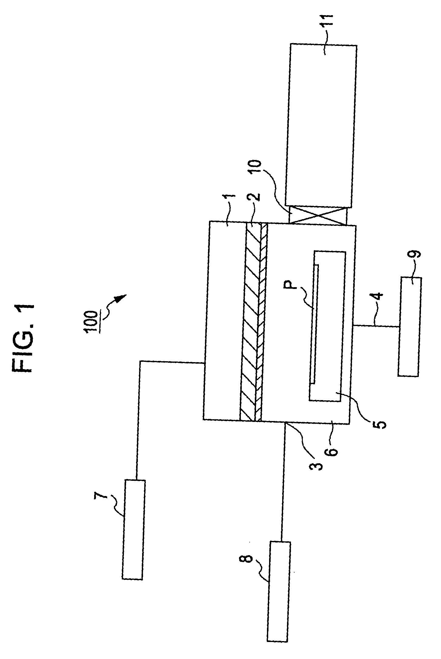
[0062] For the sample thus obtained, surface treatment was performed using the treatment apparatus 100 shown in FIG. 1.

[0063] While the temperature of the heater stage 5 receiving the sample was heated to 280° C., and deuterium (D2) was supplied as a process gas, the pressure inside the process chamber 6 was controlled to 66.7 Pa using exhaust means 9.

[0064] While the conditions described above were maintained, a microwave having a wavelength of 2.45 GHz was generated at an output of 3 ...

experimental example 2

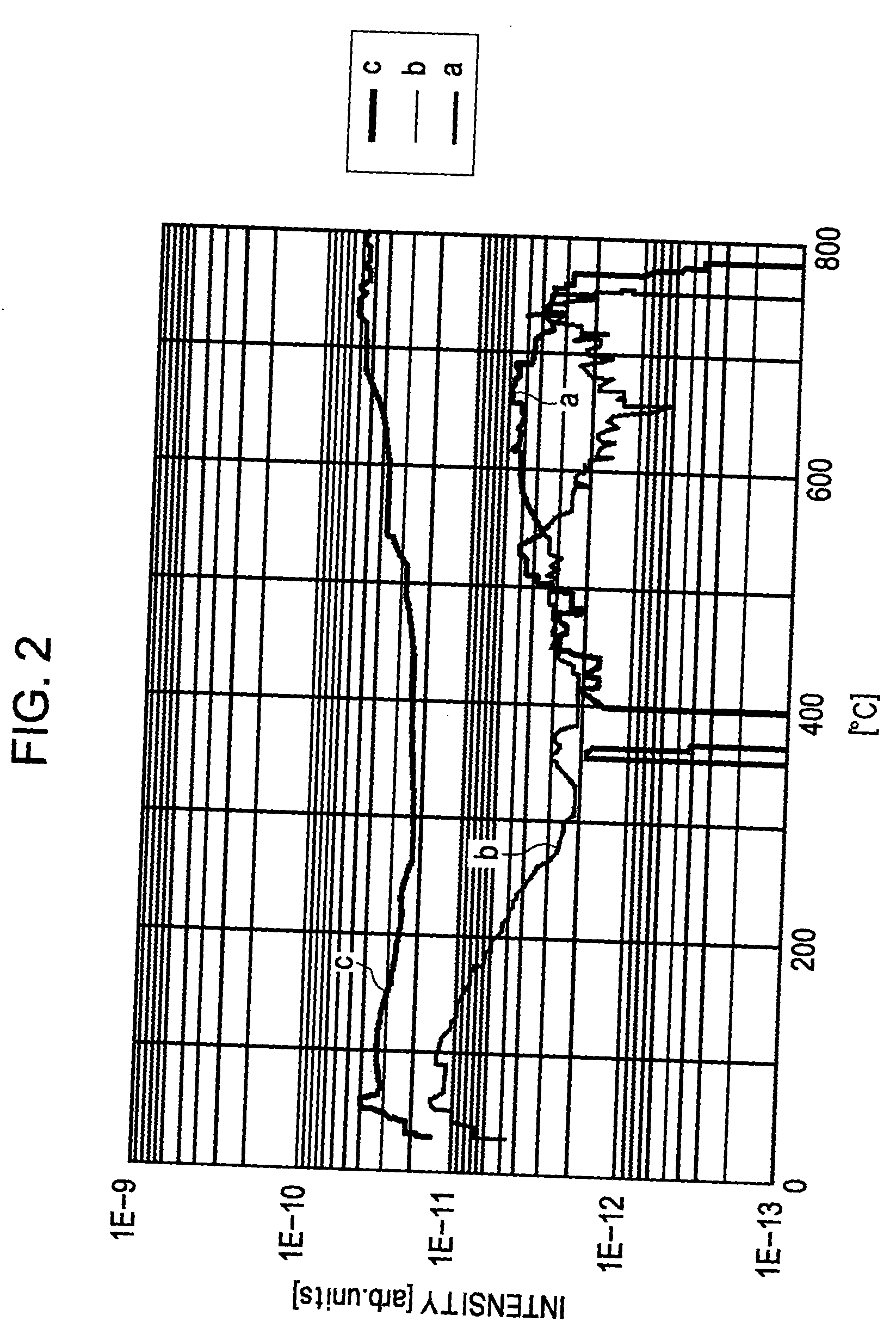
[0093] As the object, two types of monocrystal silicon wafers were prepared from wafers each provided with a native oxide film. That is, one type of wafer was prepared from a wafer provided with a native oxide film by surface treatment with deuterium plasma, followed by nitridation with nitrogen plasma. For preparing the other type of wafer, a wafer provided with a native oxide film was nitrided with nitrogen plasma without performing hydrogen plasma treatment and deuterium plasma treatment. As the plasma nitridation conditions, the microwave electrical power was 3 kW, the pressure was 2×10⁻² Pa, and the wafer temperature was 280° C.

[0094] Those two types of samples were analyzed by secondary ion mass spectrometry (SIMS), and the results are shown in FIGS. 3 and 4.

[0095] According to a sample C2 which was not surface-treated with deuterium plasma, nitridation was performed while moisture was adsorbed on the native oxide film formed on the wafer surface as shown in FIG. 3. During p...

embodiment 1

[0098] Embodiment 1 of the present invention relates to a method for manufacturing a semiconductor device, the method comprising the steps of performing surface treatment of surfaces of active regions made of monocrystalline silicon by hydrogen plasma, then performing nitridation treatment by nitrogen plasma, and subsequently forming a dielectric film having a high dielectric constant.

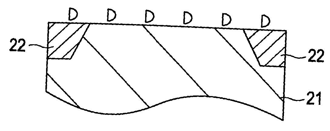
[0099] On a surface of a p-type monocrystalline silicon wafer 21 used as an object, an element isolation region 22 and an active region surrounded thereby are formed by selective oxidation or shallow trench isolation.

[0100] Next, after a native oxide film on the active region surface is removed by hydrogen fluoride anhydride, washing is performed for several seconds with purified water, so that a monocrystalline silicon surface of the active region is terminated with fluorine.

[0101] Subsequently, the object is transferred into the apparatus shown in FIG. 1, and plasma is generated by introducing a d...


PUM


Abstract

A method for processing an object containing moisture is provided to efficiently remove the moisture and to prevent re-adsorption of the moisture. In particular, the method has a step of removing the moisture contained in the object in an atmosphere containing excited hydrogen, deuterium, deuterated hydrogen, or tritium.

Description

BACKGROUND OF THE INVENTION [0001] 1. Field of the Invention [0002] The present invention relates to a surface treatment method, a manufacturing method of a semiconductor device, and a manufacturing method of a capacitive element, and more particularly, relates to a manufacturing method of a capacitive element and a manufacturing method of a MOS transistor, a CCD, a TFT, an SOI substrate, an inkjet head, and the like. [0003] 2. Description of the Related Art [0004] A semiconductor device is manufactured by sequentially performing various treatment processes for a substrate such as silicon, sapphire, or glass. The treatment processes mentioned above include, for example, cleaning, oxidation, thin-film formation, dopant doping, and etching. [0005] Treatment apparatuses used for various treatment processes are disposed in a clean room, and all the treatment processes are performed in the clean room. During the treatment processes, a semiconductor substrate is exposed to a clean room at...

Claims


Application Information

Patent Timeline
Patent Type & Authority Applications(United States)
IPC IPC(8): H01L21/31H01L29/76
CPCB41J2/1603B41J2/1606B41J2/1623B41J2/1628B41J2/1629H01L21/02046H01L29/7833H01L21/02068H01L21/28202H01L21/306H01L29/513H01L29/518H01L29/6659H01L21/0206
Inventor ISHIHARA, SHIGENORIKAWASE, NOBUO
Owner CANON KK
Why Eureka
Try Eureka