Nonvolatile memory device including nano dot and method of fabricating the same

a memory device and nano dot technology, applied in the direction of semiconductor devices, electrical devices, nanotechnology, etc., can solve the problems of affecting and requiring a relatively long fabrication time, so as to improve the reliability of the memory device

Inactive Publication Date: 2007-04-26
SAMSUNG ELECTRONICS CO LTD
View PDF5 Cites 43 Cited by
  • Summary
  • Abstract
  • Description
  • Claims
  • Application Information

AI Technical Summary

Benefits of technology

[0016] Example embodiments provide a nonvolatile memory device having a decreased and stabilized reset current value and a stabilized set voltage, thereby improving the reliability of the memory device, the memory device including an oxide layer formed of a resistance-changing material.

Problems solved by technology

Because DRAM is a volatile memory device, stored data may be lost when the power is turned off.
Unlike DRAMs, flash memory may be nonvolatile, but it may have relatively low integration density and relatively slow operating speed, compared to DRAMs.
When PRAM is fabricated by using a conventional semiconductor device fabrication process, etching may be difficult and a relatively long fabrication time may be required.
The unit cost of a product may increase due to relatively low productivity, thereby decreasing price competitiveness.
Such unstable results may be the result of the irregular current path distribution in the oxide layer 12.
When the RC value is unstable and relatively high, the reliability of the semiconductor memory device may be relatively low and power consumption may increase.

Method used


Image

  • Nonvolatile memory device including nano dot and method of fabricating the same
  • Nonvolatile memory device including nano dot and method of fabricating the same
  • Nonvolatile memory device including nano dot and method of fabricating the same

Examples


Embodiment Construction

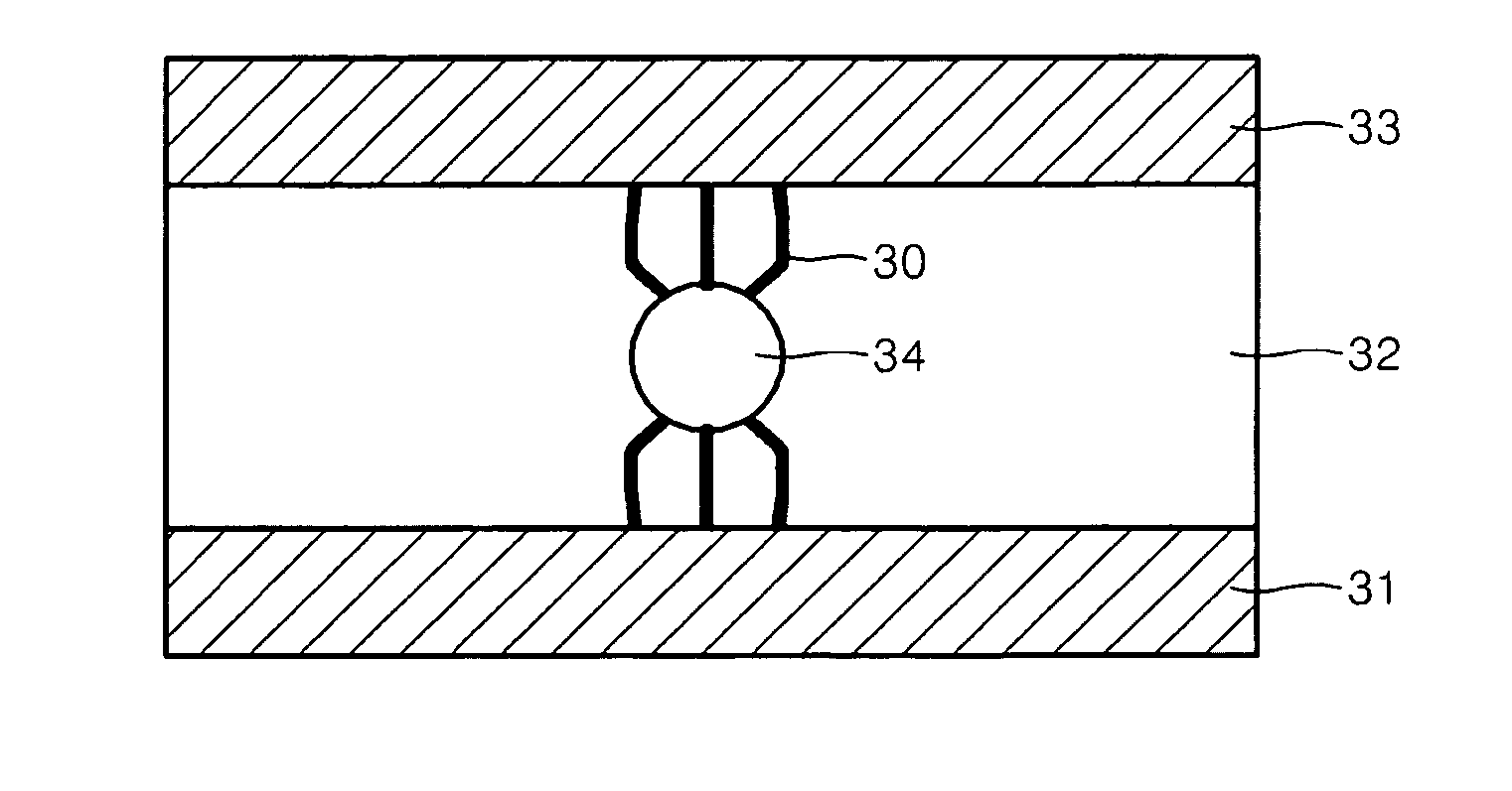
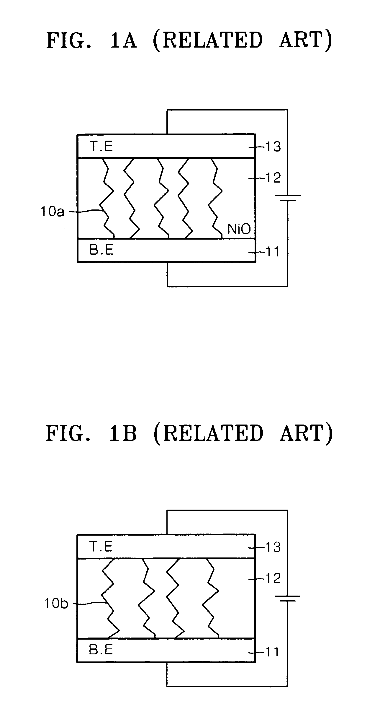
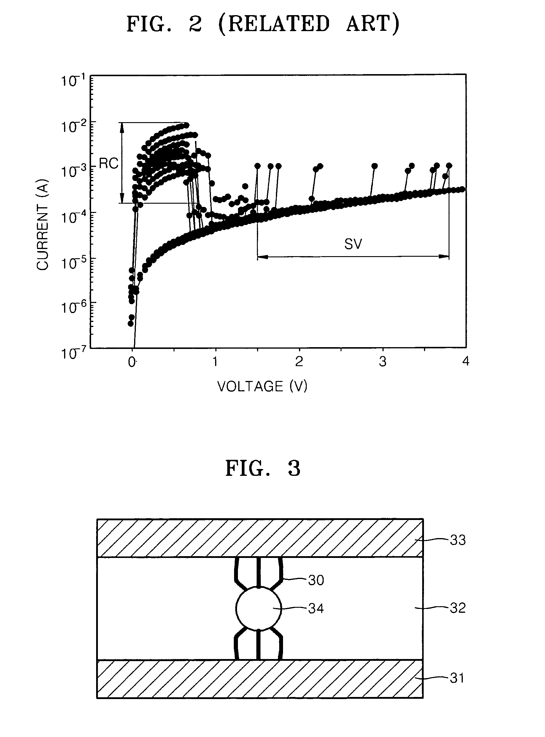
[0032] A nonvolatile memory device including a nano dot and a method of fabricating the same will now be described more fully hereinafter with reference to the accompanying drawings, in which example embodiments are shown. In the drawings, the thickness of layers and regions are exaggerated for clarity.

[0033] Spatially relative terms, such as “beneath,”“below,”“lower,”“above,”“upper” and the like, may be used herein for ease of description to describe one element or feature's relationship to another element(s) or feature(s) as illustrated in the figures. It will be understood that the spatially relative terms are intended to encompass different orientations of the device in use or operation in addition to the orientation depicted in the figures. For example, if the device in the figures is turned over, elements described as “below” or “beneath” other elements or features would then be oriented “above” the other elements or features. Thus, the example term “below” may encompass both...


PUM

PropertyMeasurementUnit
voltageaaaaaaaaaa
currentaaaaaaaaaa
resistanceaaaaaaaaaa

Abstract

A nonvolatile memory device including a nano dot and a method of fabricating the same are provided. The nonvolatile memory device may include a lower electrode, an oxide layer on the lower electrode, a nano dot in the oxide layer and an upper electrode on the oxide layer. In example embodiments, the current paths inside the oxide layer may be unified, thereby stabilizing the reset current.

Description

PRIORITY STATEMENT [0001] This application claims the benefit of Korean Patent Application No. 10-2005-0099737, filed on Oct. 21, 2005, in the Korean Intellectual Property Office, the disclosure of which is incorporated herein in its entirety by reference. BACKGROUND [0002] 1. Field [0003] Example embodiments relate to a nonvolatile memory device and a method of fabricating the same. Other example embodiments relate to a nonvolatile memory device including an oxide layer having a resistance gradient, which unifies current paths in the oxide layer by forming a nano dot in the oxide layer, and a method of fabricating the same. [0004] 2. Description of the Related Art [0005] Research has been conducted to enhance the integration density of semiconductor devices, for example, semiconductor memory devices. As the integration density is enhanced, the memory capacity per unit area of the memory devices may be improved. Research has also been conducted on driving the device at relatively lo...

Claims


Application Information

Patent Timeline
Patent Type & Authority Applications(United States)
IPC IPC(8): H01L29/76H01L21/8238
CPCH01L27/101H01L27/115H01L45/04H01L45/1233H01L45/1246H01L45/146H01L45/1608H01L27/2436H01L27/1052H10B63/30H10N70/20H10N70/828H10N70/826H10N70/8833H10N70/021H10B99/00H10B69/00B82Y10/00
Inventor PARK, SANG-JINLEE, MYOUNG-JAECHA, YOUNG-KWANSEO, SUN-AECHO, KYUNG-SANGSEOL, KWANG-SOO
Owner SAMSUNG ELECTRONICS CO LTD
Why Eureka
Try Eureka