Liquid crystal display device

a liquid crystal display and display device technology, applied in non-linear optics, instruments, optics, etc., can solve the problems of increasing the cost of manufacturing liquid crystal display devices, increasing the amount of liquid crystal wasted during the liquid crystal injection process, and difficulty in dropping adequate amount of liquid crystal, so as to prevent undesirable gravity mura phenomenon, reduce the viscosity of liquid crystal, and prevent undesirable gravity mura

Inactive Publication Date: 2007-04-26
AU OPTRONICS CORP
View PDF3 Cites 4 Cited by
  • Summary
  • Abstract
  • Description
  • Claims
  • Application Information

AI Technical Summary

Benefits of technology

[0012] Therefore, a space (buffer region) for receiving the overflowing liquid crystal is formed outside the display region. Besides, due to the height of the rampart is smaller than the cell gap between the upper substrate and the lower substrate of the liquid crystal device, there is a gap between the rampart and the upper substrate (or the lower substrate) or between two ramparts formed on the surface of the upper substrate and on the surface of the lower substrate respectively. The liquid crystal inside the display region can overflow into the space inside the buffer region through the gap. Therefore, the level of the liquid crystal inside the display region can be properly controlled, and the cell gap between the upper substrate and the lower substrate of the liquid crystal display device of the present invention can be maintained by the spacer thereinbetween, not the liquid crystal thereinbetween. Thus, the undesirable “gravity mura” phenomenon can be prevented. Moreover, since the space (buffer region) between the rampart and the sealing member is vacuumed and its pressure is much less than that of the space inside the active region, the overflowing liquid crystal flowing into the buffer region will not flow back into the active region again.
[0013] Furthermore, since the spacer of the liquid crystal display device of the present invention is formed on the sides of the upper substrate and the lower substrate, and the viscosity of the liquid crystal will be lowered if it's heated. When an additional “heat and spin” process is executed after the Vacuum Pressure Annealing (VPA) process, the overflowing liquid crystal will flow into the space between the rampart and the sealing member. As a result, the spacer can maintains the cell gap of the liquid crystal display device of the present invention. And the level of the liquid crystal inside the display region can be properly controlled. At the same time, the undesirable “gravity mura” phenomenon can also be prevented.
[0017] As a result, the level of the liquid crystal inside the display region of the liquid crystal display device of the present invention can be properly controlled and the undesirable “gravity mura” phenomenon can be prevented. Besides, the cell gap of the liquid crystal display device of the present invention is well maintained and the yield of the liquid crystal display device of the present invention is raised significantly.

Problems solved by technology

Moreover, the amount of the liquid crystal wasted during the liquid-crystal-injecting process also increases.
Hence the cost for manufacturing liquid crystal display devices increases.
However, it is difficult to drop adequate amount of liquid crystal to match the critical amount for maintaining the height that the spacer is.
In fact, the disadvantage of excessive injection of liquid crystal always happens in ODF process so far.
These undesirable bubbles will deteriorate the performance of the liquid crystal display device, such as the brightness or the response time.
As a result, the spacer cannot define the cell gap 3 inside the liquid crystal display device.
That is, the thickness of the panel of the liquid crystal display device is not consistent over the whole area of the liquid crystal display device.

Method used


Image

  • Liquid crystal display device
  • Liquid crystal display device
  • Liquid crystal display device

Examples


Embodiment Construction

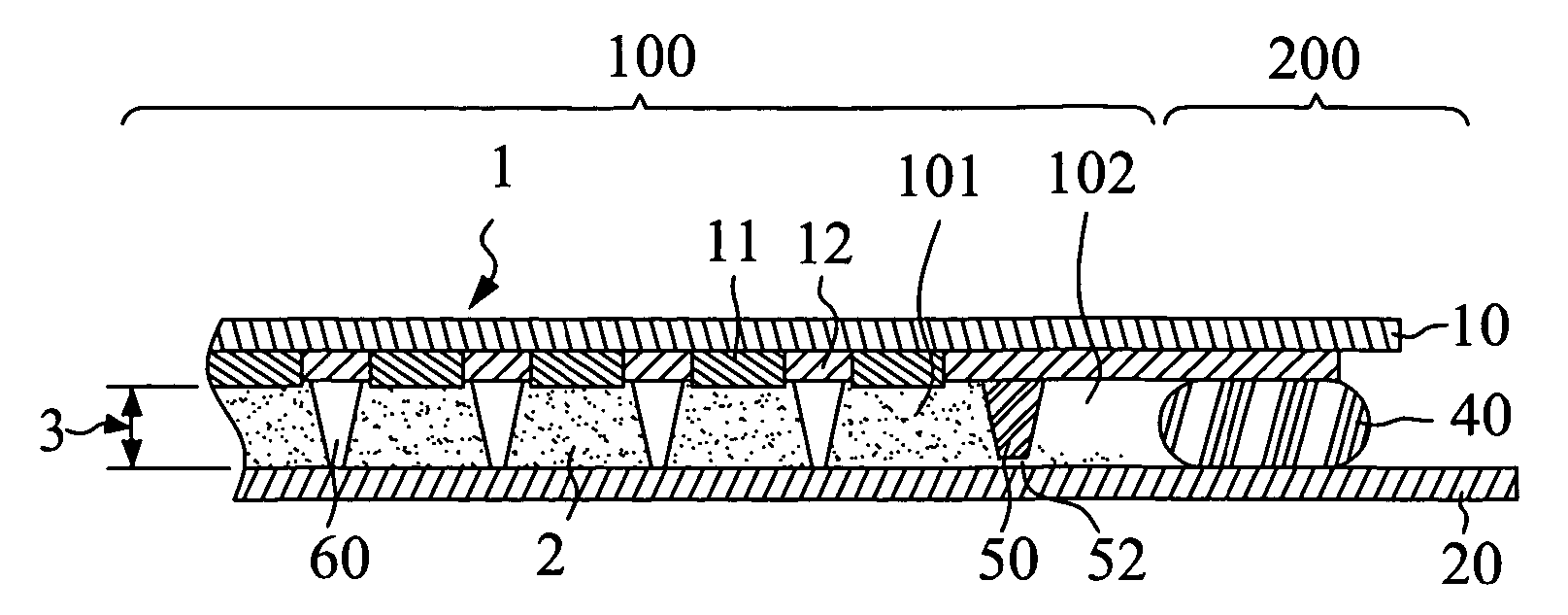
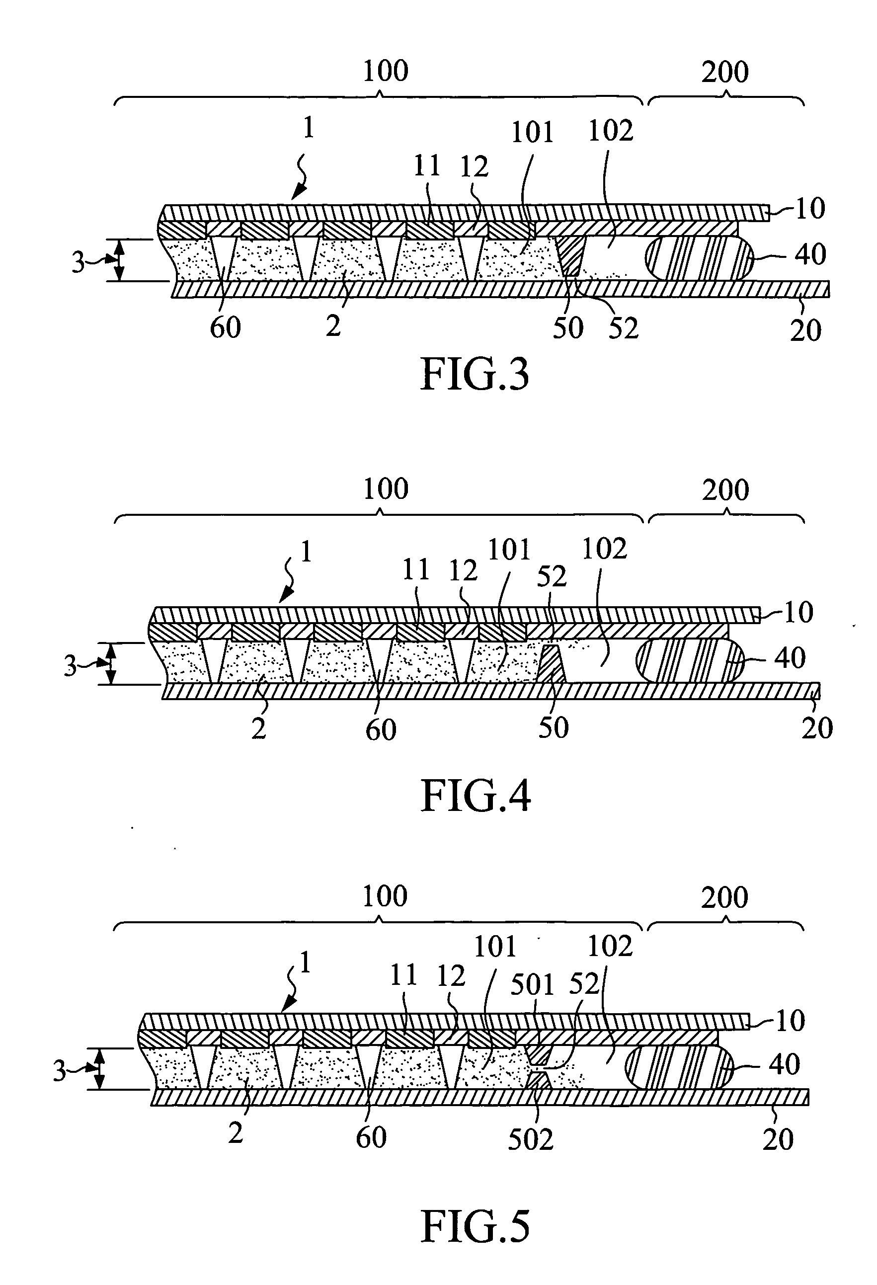
[0029] Please refer to FIG. 3, which is a cross section view of the liquid crystal display device of the first preferred embodiment of the present invention. The rampart 50 and the sealing member 40 are formed on the upper surface of the lower substrate 20. The sealing member 40 divides the space between the upper substrate 10 and the lower substrate 20 into a center region 100 and a peripheral region 200, while the rampart 50 divides the center region 100 into a display region 101 and a buffer region 102. The sealing member 40 seals the center region 100 and the liquid crystal is filled inside the display region 101. A plurality of pigment layers 11, a plurality of shielding layers 12, a plurality of spacers 60 and at least one rampart 50 are formed on a surface of the upper substrate 10. The pigment layers 11 are color filter sheets and the shielding layers 12 are black matrices, while the spacers 60 are formed inside the display region 101. Since the rampart 50 and the spacers 60...


PUM

PropertyMeasurementUnit
heightaaaaaaaaaa
heightsaaaaaaaaaa
pressureaaaaaaaaaa

Abstract

A liquid crystal display device is disclosed, which comprises a upper substrate; a lower substrate; a liquid crystal layer; a sealing member sandwiched between the upper substrate and the lower substrate; and at least one rampart. The sealing member divides the space between the upper substrate and the lower substrate into a center region inside the sealing member and a peripheral region outside the sealing member. The rampart positioned in the center region divides the center region into a display region and a buffer region. The height of the rampart is smaller than the cell gap between the upper substrate and the lower substrate. Therefore, the level of the liquid crystal inside the display region can be properly controlled and the undesirable “gravity mura” phenomenon can be prevented.

Description

BACKGROUND OF THE INVENTION [0001] 1. Field of the Invention [0002] The present invention relates to a liquid crystal display device and, more particularly, to a liquid crystal display device suitable for filling liquid crystal by one-drop fill-method (ODF). [0003] 2. Description of Related Art [0004] Currently, the conventional method for filling the liquid crystal into the panel cells of a liquid crystal display device comprises following steps: (a) aligning and assembling the upper substrate and the lower substrate together to form a panel with an empty panel cell; (b) laying the panel into a vessel; (c) vacuuming the empty panel cell and immersing the panel into the vessel filled with liquid crystal; and (d) injecting the liquid crystal into the empty panel cell by the assistance of pressure difference and capillary effect. [0005] But when the size of the panel of a liquid crystal display device becomes larger, as the evolution from the 5.5-th Generation glass substrate to the 7...

Claims


Application Information

Patent Timeline
Patent Type & Authority Applications(United States)
IPC IPC(8): G02F1/1339
CPCG02F1/1341G02F2001/133388G02F2001/13396G02F1/133388G02F1/13396
Inventor CHANG, CHIH-CHIEHWU, PIN-CHUN
Owner AU OPTRONICS CORP
Why Eureka
Try Eureka