Semiconductor device with vertical electron injection and its manufacturing method

a semiconductor and electron injection technology, applied in semiconductor laser excitation apparatus, semiconductor laser structure details, lasers, etc., can solve the problems of very expensive sic substrates, difficult or even impossible to obtain solid substrates in semiconductor extremely difficult or even impossible to obtain semiconductor solid substrates with a big gap, etc., to achieve less expensive

Inactive Publication Date: 2007-04-26
COMMISSARIAT A LENERGIE ATOMIQUE ET AUX ENERGIES ALTERNATIVES
View PDF12 Cites 25 Cited by
  • Summary
  • Abstract
  • Description
  • Claims
  • Application Information

AI Technical Summary

Benefits of technology

[0015] The present invention proposes a new device that can be less costly than prior art solutions, for obtaining a semiconductor device with vertical electron injection.
[0018] Possibly, the device can furthermore comprise a layer called an adhesion layer, situated between the support substrate and the structure and making it possible to solidify the monocrystalline thin film on the support, the adhesion layer allowing electric or electronic access to the electronic component. This adhesion layer can be in SiO2.

Problems solved by technology

At present it is extremely difficult or even impossible to obtain solid substrates in a semiconductor with a big gap.
Nonetheless, epitaxy of GaN on sapphire is made particularly delicate because of the difference in lattice structure existing between GaN and sapphire (of the order of 16%).
SiC substrates remain rare and very expensive.
Other methods are also being studied, but their present state of development restricts them to laboratory use.
Apart from the problem of producing epitaxial GaN, the first epitaxy of SiC poses significant technical problems.
This approach, based on a principle equivalent to that adopted for epitaxy on sapphire, suffers at present from being far behind, relative to other techniques.
Furthermore, the nature of the substrate chosen for epitaxy has an influence on the performance of the device via the problem of heat dissipation during operation.
The limitations recognized concerning devices produced on GaN supported by sapphire, are under study at present.

Method used


Image

  • Semiconductor device with vertical electron injection and its manufacturing method
  • Semiconductor device with vertical electron injection and its manufacturing method
  • Semiconductor device with vertical electron injection and its manufacturing method

Examples


Embodiment Construction

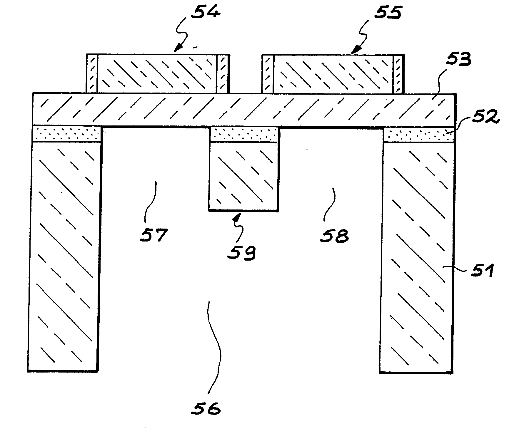
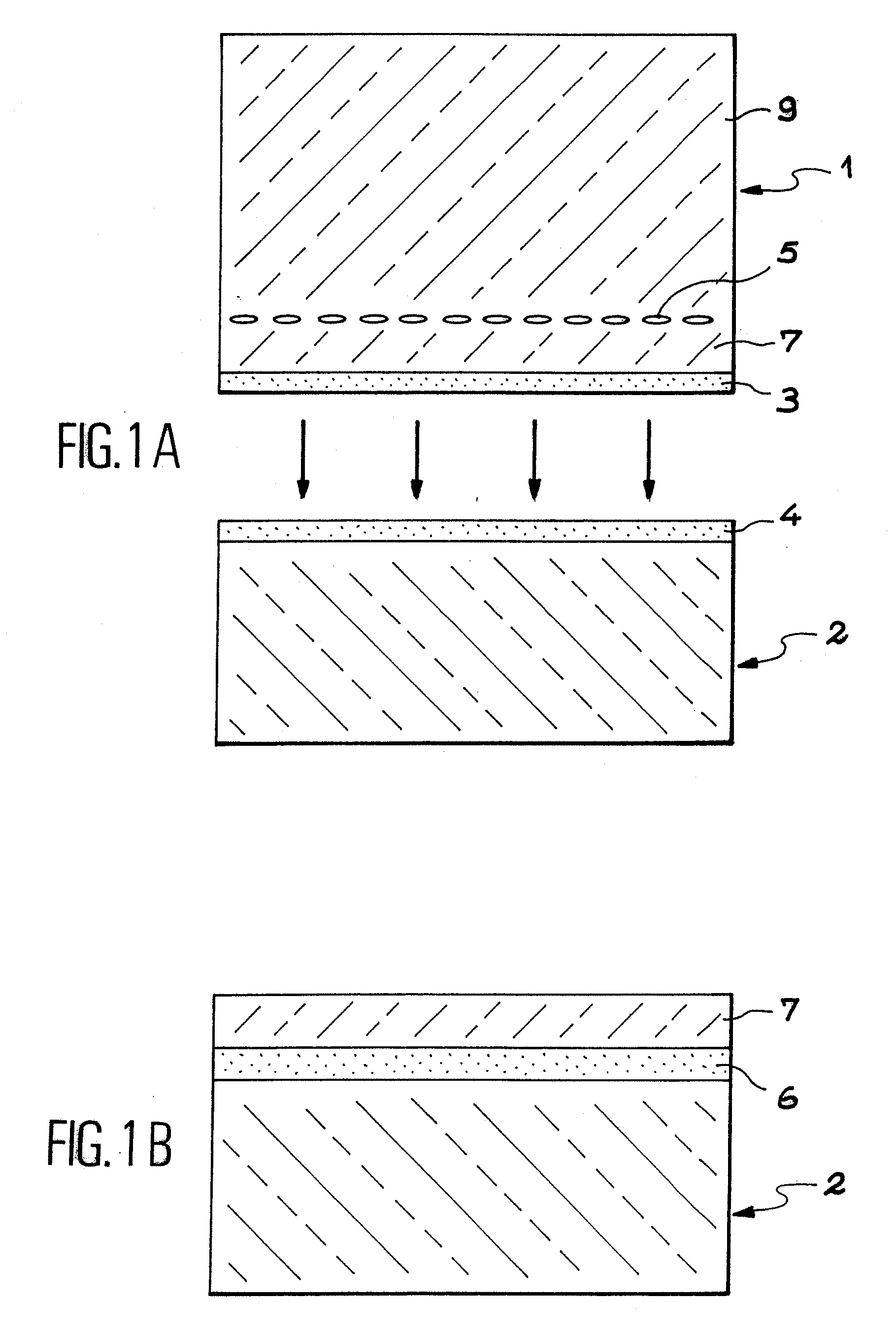
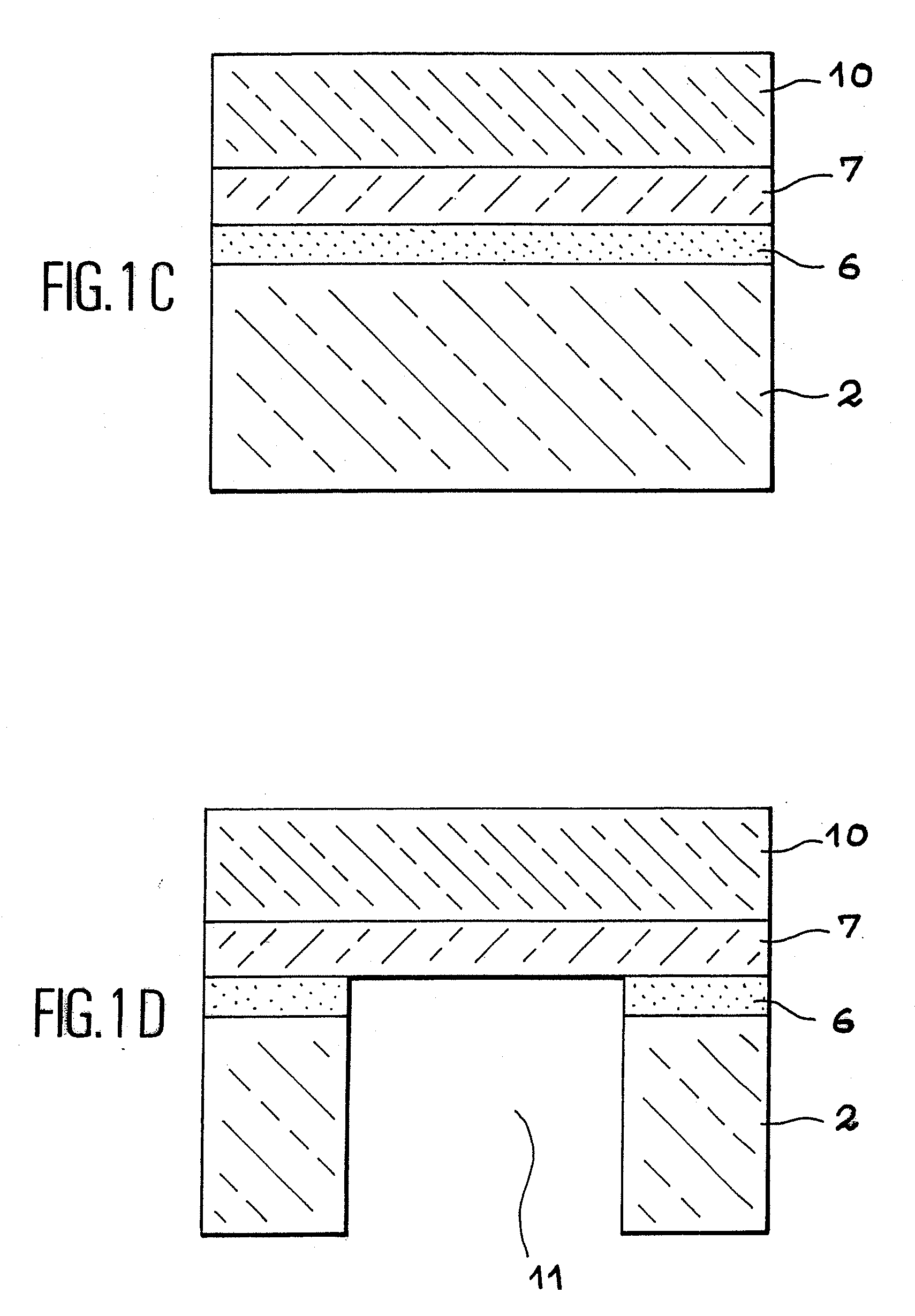
[0048] The manufacture of a semiconductor device with vertical electron injection according to the invention comprises the transfer of a monocrystalline thin film of very high crystalline quality (semiconducting or not, insulating or electrically conducting) onto the front face of a substrate, semiconducting or not. This transfer can be carried out through the intermediary of an insulating thin film, metallic or semiconducting. The required active layer or layers are obtained by crystal growth before or after transfer. One or several electronic components are thus formed. The rear face of the substrate is machined or micro-machined locally in order to create a membrane. The monocrystalline thin film can possibly be thinned.

[0049] According to an embodiment of the invention, the active layer and the monocrystalline thin film form a single and same layer.

[0050] The electronic component or components can be manufactured before or after the formation of the membrane. Nonetheless, it i...


PUM


Abstract

A method for making a semiconductor device with vertical electron injection, including: transferring a monocrystalline thin film onto a first face of a support substrate; producing at least one electronic component from the monocrystalline thin film; forming at least one recess in a second face of the substrate to enable electric or electronic access to the electronic component through the monocrystalline thin film; and producing a vertical electron injector configured to inject electrons into the electronic component.

Description

CROSS REFERENCE TO RELATED APPLICATIONS [0001] This application is a divisional of U.S. application Ser. No. 10 / 276,691, filed Nov. 18, 2002, and is based upon and claims the benefit of priority to WIPO Application No. PCT / FR01 / 01603, filed May 23, 2001 and from the prior French Patent Application No. 00 / 06761, filed on May 26, 2000, the entire contents of each of which are incorporated herein by reference.FIELD OF THE INVENTION [0002] The present invention relates to a semiconductor device with vertical electron injection. It also concerns a manufacturing method for such a device. [0003] The semiconductor device with vertical electron injection is produced in an active layer in semiconducting material with a small gap or a big gap. However, the invention proves to be of particular interest in the case of an active layer in semiconducting material with a big gap. BACKGROUND OF THE INVENTION [0004] Semiconductors are characterized by their forbidden band or gap separating the last fi...

Claims


Application Information

Patent Timeline
Patent Type & Authority Applications(United States)
IPC IPC(8): H01L21/338H01L21/20H01L21/36H01J31/00H01L33/00H01L33/20H01S5/02H01S5/04H01S5/042H01S5/10H01S5/183H01S5/30H01S5/323
CPCH01J31/00H01L33/007H01L2924/0002H01L33/0079H01L33/20H01S3/0959H01S5/021H01S5/0215H01S5/0217H01S5/04H01S5/0425H01S5/10H01S5/3013H01S5/32341H01L2924/00H01S5/04254H01S5/0207H01L33/0093
Inventor BAPTIST, ROBERTLETERTRE, FABRICE
Owner COMMISSARIAT A LENERGIE ATOMIQUE ET AUX ENERGIES ALTERNATIVES
Why Eureka
Try Eureka