Gallium nitride-based compound semiconductor light-emitting device and negative electrode thereof

Active Publication Date: 2007-05-03
TOYODA GOSEI CO LTD
2 Cites 8 Cited by

AI-Extracted Technical Summary

Problems solved by technology

Through employment of such a compound semiconductor, ultraviolet light, blue light, or green light of high emission intensity can be obtained; such high-intensity light has conventionally been difficult to attain.
Unlike the case of a GaAs light-emitting device, such a gallium nitride-based compound semiconductor is generally grown on a sapphire s...

Benefits of technology

[0035] The negative electrode according to the present invention has a contact metal layer comprising a Cr—Al alloy. Thus, the negative electrode attains excellent Ohmic contact with an n-type gallium nitride-based compound semiconductor layer and is not deteriorated, in characteristics, by heating. Such an excellent Ohmic con...

Abstract

An object of the present invention is to provide a negative electrode which attains excellent Ohmic contact with an n-type gallium nitride-based compound semiconductor layer, which resists deterioration in characteristics which would be caused by heating, and which can be produced at high efficiency. Another object of the invention is to provide a gallium nitride-based compound semiconductor light-emitting device having the negative electrode. The inventive gallium nitride-based compound semiconductor light-emitting device comprises an n-type semiconductor layer of a gallium nitride-based compound semiconductor, a light-emitting layer of a gallium nitride-based compound semiconductor and a p-type semiconductor layer of a gallium nitride-based compound semiconductor formed on a substrate in this order, and has a negative electrode and a positive electrode provided on the n-type semiconductor layer and the p-type semiconductor layer, respectively; wherein the negative electrode comprises a bonding pad layer and a contact metal layer which is in contact with the n-type semiconductor layer, and the contact metal layer is composed of a Cr—Al alloy.

Application Domain

Solid-state devicesSemiconductor/solid-state device manufacturing +1

Technology Topic

Gallium nitrideOhmic contact +4

Image

  • Gallium nitride-based compound semiconductor light-emitting device and negative electrode thereof
  • Gallium nitride-based compound semiconductor light-emitting device and negative electrode thereof

Examples

  • Experimental program(1)

Example

[0038] In the present invention, no particular limitations are imposed on the gallium nitride-based compound semiconductor layers stacked on a substrate, so long as the semiconductor stacked layers have a structure as shown in FIG. 1; i.e., a stacked structure including a buffer layer 2, an n-type semiconductor layer 3, a light-emitting layer 4, and a p-type semiconductor layer 5, the layers being formed atop a substrate 1 through crystal growth. No particular limitation is imposed on the type of the substrate, and any conventionally known substrate, such as a sapphire substrate or an SiC substrate, may be employed. No particular limitation is imposed on the type of the gallium nitride-based compound semiconductor, and conventionally known gallium nitride-based compound semiconductors represented by formula: AlxGayIn1-x-yN (0≦x ≦1, 0≦y≦1, x+y≦1) may be employed.
[0039]FIG. 2 shows one exemplary employable stacked structure in which an AlN buffer layer 2, an n-type GaN contact layer 3a, an n-type GaN lower cladding layer 3b, an InGaN light-emitting layer 4, a p-type AlGaN upper cladding layer 5b, and a p-type GaN contact layer 5a are sequentially stacked on a sapphire substrate 1. No particular limitation is imposed on the composition and structure of a positive electrode 10 to be provided atop the contact layer 5a, and a positive electrode having a conventional composition and structure (e.g., Al) may be employed.
[0040] A portion of the contact layer 5a, that of the upper cladding layer 5b, that of the light-emitting layer 4, and that of the lower cladding layer 3b, these layers being formed of the aforementioned gallium nitride-based compound semiconductor, are removed through etching, and a negative electrode 20 is provided on the thus-exposed portion of the contact layer 3a. The negative electrode 20 is constituted of a contact metal layer 21, an adhesion layer 22, and a bonding pad layer 23.
[0041] According to the present invention, the negative electrode at least contains layers; i.e., a contact metal layer which is in Ohmic contact with an n-type semiconductor layer, and a bonding pad layer for establishing electric contact with a circuit substrate, a lead frame, etc., and the contact metal layer is composed of a Cr—Al alloy. As the contact metal layer is formed of a Cr—Al alloy, thermally induced deterioration, in characteristics, can be prevented. Thus, a negative electrode which has a low contact resistance and which can be produced with high efficiency can be obtained.
[0042] The contact metal layer preferably has a thickness of 1 nm or more. A layer thickness of 5 nm or more is particularly preferred, from the viewpoint of attainment of low resistance. The thickness is more preferably 10 nm or more, as a constant low resistance can then be attained. However, when the thickness is excessively large, productivity decreases. Thus, the thickness is preferably 500 nm or less, more preferably 200 nm or less.
[0043] The Cr content of the Cr—Al alloy is preferably 10 to 90 mass %. Particularly when thermal-induced deterioration in characteristics of the light-emitting device is to be prevented, the Cr content is preferably controlled to 20 to 80 mass %. In order to more reliably prevent deterioration in characteristics, the Cr content is preferably controlled to 40 to 60 mass %. The Al content of the alloy is preferably 90 to 10 mass %, more preferably 80 to 20 mass %, particularly preferably 60 to 40 mass %. In a small amount of about 10 mass % or less, the alloy may contain a metal other than Cr and Al. Examples of the metal to be incorporated into the alloy include V, Nb, Mo, and W. Also, as the reflectivity of Cr becomes higher after heating at 300° C., it is preferable that the Cr content is high.
[0044] The contact resistance between the contact metal layer and an n-type GaN semiconductor layer is greatly affected by the degree of removal of oxide film formed spontaneously on the surface of the n-type GaN semiconductor layer. The surface of the GaN semiconductor layer is oxidized in the atmosphere, thereby forming natural oxide film. Even in the case where the thus-formed oxide film is removed through etching or similar means, the surface is oxidized again, if the surface is exposed to the atmosphere before formation of an electrode. As the oxide film formed on GaN serves as an insulator, the contact resistance at the interface between the electrode and GaN increases, if the entire GaN surface is covered with the oxide film. Therefore, removal of oxide film formed on the surface of an n-type semiconductor layer before formation of the contact metal layer is a key issue.
[0045] The bonding pad layer is preferably formed of a metal selected from the group consisting of Au, Al, Ni, and Cu, or formed of an alloy containing the metal, from the viewpoint of attainment of good contact with a bump. The bonding pad layer preferably has a thickness of 100 to 1,000 nm, from the viewpoint of productivity. The thickness is preferably 200 to 800 nm, particularly preferably 200 to 500 nm.
[0046] In order to improve adhesion between the contact metal layer and the bonding pad layer, an adhesion layer formed of Ti preferably intervenes between the two layers. The adhesion layer, if employed, preferably has a thickness of 1 to 100 nm. When the thickness is less than 1 nm, the effect of adhesion is poor, whereas when the thickness is more than 100 nm, the Ti film is oxidized in the case where the light-emitting device is in a heated state, and in some cases, the electrical characteristics may be impaired. From the viewpoint of reliable adhesion effect, a thickness of 5 nm or more is preferred, with 10 nm or more being particularly preferred.
[0047] An Au—Sn alloy layer or a lead free solder layer can be preferably provided on the bonding pad layer. This layer functions as an adhesion layer in order to adhere the light-emitting device to a sub-mount. This layer preferably has a thickness of 200 nm or more, from the viewpoint of attaining the adhesion. Also, this layer preferably has a thickness of 5 μm or less, from the viewpoint of productivity.
[0048] Even in a case of providing the Au—Sn alloy layer or the lead free solder layer, a negative electrode is heated to 300˜400° C. for some minutes during mounting. By the heat generated during mounting, a Cr atom in the contact metal layer may diffuse to the bonding pad layer and the Au—Sn alloy layer or the lead free solder layer.
[0049] Therefore, in order to prevent the Cr diffusion, a barrier layer can be preferably provided between the contact metal layer and the bonding pad layer or between the bonding pad layer and the Au—Sn alloy layer or the lead free solder layer. The barrier layer is preferably formed of a metal selected from the group consisting of Ti, Zr, Hf, Ta, W, Re, Os, Ir, Pt, Fe, Co, Ni, Ru, Rh, and Pd, or formed of an alloy containing the metal. Among these metals, Ti, Ta, W, and Pt are more preferable. The barrier layer preferably has a thickness of 10 nm or more, from the viewpoint of forming a uniform single layer. Also, it preferably has a thickness of 500 nm or less, from the viewpoint of productivity. The thickness is more preferably 50 to 300 nm.
[0050] When the above-mentioned adhesion layer of Ti is provided, it also functions as the barrier layer.
[0051] No particular limitation is imposed on the method of forming the contact metal layer, the bonding pad layer, the adhesion layer and the barrier layer, and any conventionally known method such as sputtering or vapor deposition may be employed. The same single method may be employed to form the respective layers, or methods different from one another may be employed. However, formation of all the layers through a single common method is preferred for the purpose of simplifying the steps. Also, no particular limitation is imposed on the method of forming the Au—Sn alloy layer or the lead free solder layer, and any conventionally known method such as vapor deposition, plating and a coating method using a paste, may be employed.
[0052] The present inventive gallium nitride-based compound semiconductor light-emitting device can preferably form a lamp.
EXAMPLES
[0053] The present invention will next be described in more detail by way of Examples and Comparative Examples. Table 1 shows negative electrode materials employed in the Examples and Comparative Examples, and evaluation of characteristics immediately after formation of a negative electrode film and after a heating test. Needless to say, these Examples and Comparative Examples should not be construed as limiting the invention.
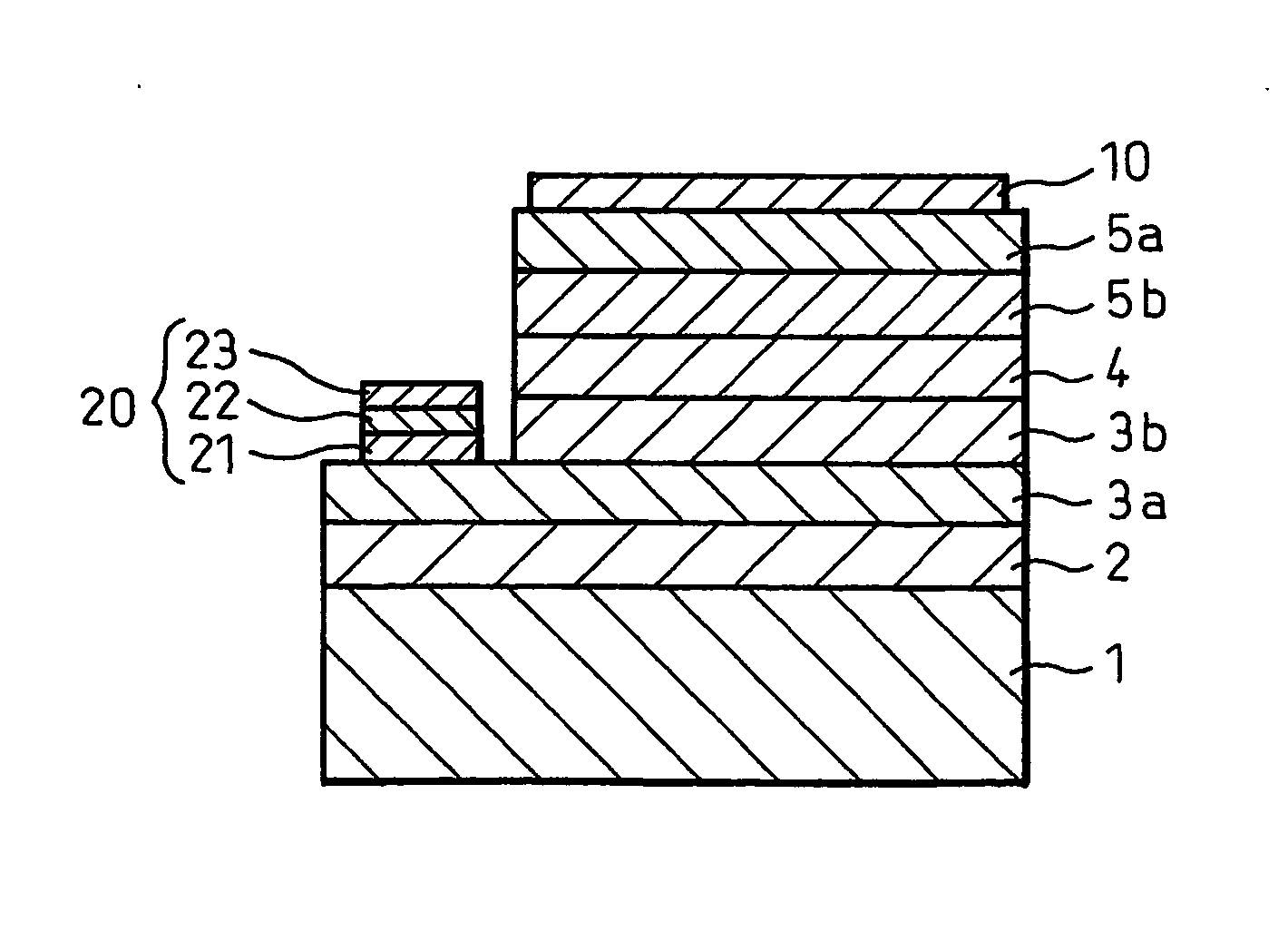
[0054]FIG. 2 is a schematic view showing a gallium nitride-based compound semiconductor light-emitting device produced in the present Example.
[0055] The gallium nitride-based compound semiconductor stacked structure employed for fabricating the light-emitting device was produced through the following procedure: an AlN buffer layer 2 was formed on a sapphire substrate 1; and an n-type GaN contact layer 3a, an n-type GaN lower cladding layer 3b, an InGaN light-emitting layer 4, a p-type AlGaN upper cladding layer 5b, and a p-type GaN contact layer 5a were successively formed atop the buffer layer 2. The contact layer 3a is formed of n-type GaN doped with Si (7×10¹⁸/cm3), the lower cladding layer 3b is formed of n-type GaN doped with Si (5×10¹⁸/cm3), and the light-emitting layer 4, having a single quantum well structure, is formed of In0.95Ga0.05N. The upper cladding layer 5b is formed of p-type Al0.25Ga0.75N doped with Mg (1×10¹⁸/cm3). The contact layer 5a is formed of p-type GaN doped with Mg (5×10¹⁹/cm3). Stacking of these layers was performed by means of MOCVD under typical conditions which are well known in the art.
[0056] A positive electrode 10 and a negative electrode 20 were provided on the gallium nitride-based compound semiconductor stacked structure through the below-described procedure, to thereby fabricate a flip-chip-type gallium nitride-based compound semiconductor light-emitting device.
[0057] Firstly, in order to remove the oxide film on the contact layer 5a, the gallium nitride-based compound semiconductor stacked structure was treated in boiling concentrated HCl for 10 minutes.
[0058] Then, the positive electrode 10 made of Al was formed on the contact layer 5a through the following procedure. A resist was uniformly applied onto the entire surface of the contact layer, and a portion of the resist provided on the region where the positive electrode was to be formed was removed through a conventional lithographic technique. The thus-formed structure was immersed in buffered hydrofluoric acid (BHF) at room temperature for one minute, followed by forming a positive electrode in a vacuum deposition apparatus. Specifically, the thus-treated structure was placed in a vacuum deposition apparatus, and a positive electrode in the form of Al film was formed at a pressure of 4×10⁻⁴ Pa or lower through the electron beam method. The thickness of the formed film was adjusted to 100 nm. After film formation, the structure was removed from the vapor deposition apparatus, and a portion of metallic film other than the positive electrode region was removed along with the resist through a lift-off technique.
[0059] Subsequently, a negative electrode 20 was formed on the contact layer 3a through the following procedure.
[0060] Firstly, an etching mask was formed on the positive electrode through the following procedure. After uniform provision of a resist on the entire surface, a portion of the resist corresponding to a region slightly wider than the positive electrode region was removed through a conventional lithography technique. The structure was placed in a vacuum vapor deposition apparatus, and an Ni layer and a Ti layer were stacked, through the electron beam method, to thicknesses of about 50 nm and 300 nm, respectively, under a pressure of 4×10⁻⁴ Pa or lower. Thereafter, a portion of metal film other than the positive electrode region was removed along with the resist through the lift-off technique. The etching mask serves as a protective layer for protecting the positive electrode from plasma-induced damage during reactive ion dry etching.
[0061] Subsequently, the contact layer 3a was exposed, and a negative electrode was formed on the thus-exposed portion through the following procedure. Specifically, the semiconductor stacked structure was etched through reactive ion dry etching until the contact layer 3a was exposed, and the resultant stacked structure was removed from the dry etching apparatus. The aforementioned etching mask was removed by use of nitric acid or hydrofluoric acid.
[0062] After uniform provision of a resist on the entire surface, a portion of the resist corresponding to the exposed contact layer 3a region was removed through a conventional lithography technique. Subsequently, through the aforementioned vapor deposition method, a Cr20Al80 contact metal layer 21, a Ti adhesion layer 22, and an Au bonding pad layer 23 were formed at a thickness of 100 nm, 20 nm, and 300 nm, respectively. Thereafter, a portion of metal film other than the negative electrode region was removed along with the resist, thereby fabricating the gallium nitride-based compound semiconductor light-emitting device of the present invention.
[0063] In a similar manner, gallium nitride-based compound semiconductor light-emitting devices were fabricated by use of contact metal layer materials, adhesion layer materials, and bonding pad layer materials listed in Table 1. Specific contact resistance values of the thus-produced light-emitting devices were determined through the circular TLM method. The results are also shown in Table 1. TABLE 1 After film formation After heating Specific contact Specific contact Contact metal Adhesion Bonding resistance resistance layer layer pad layer Type Ω· cm2 Type Ω· cm2 1 Cr20Al80 Ti Au Ohmic 4 × 10⁻⁵ Ohmic 3 × 10⁻⁵ 2 Cr80Al20 Ti Au Ohmic 4 × 10⁻⁵ Ohmic 3 × 10⁻⁵ 3 Cr50Al50 Ti Au Ohmic 3 × 10⁻⁵ Ohmic 3 × 10⁻⁵ 4 Cr Ti Au Ohmic 3 × 10⁻⁵ Schottky 5 Cr — Au Ohmic 3 × 10⁻⁵ Schottky 6 Cr — Al Ohmic 4 × 10⁻⁵ Schottky 7 Al Ti Au Ohmic 1 × 10⁻⁵ Ohmic 8 × 10⁻⁵ 8 Cr80Ti20 Ti Au Ohmic 9 × 10⁻⁵ Schottky 9 Cr80V20 Ti Au Ohmic 1 × 10⁻⁴ Schottky 10 Cr50Pt50 Ti Au Schottky
[0064] The heating test was performed in an RTA furnace in the atmosphere at 300° C. for one minute.
[0065] When the contact metal layer is formed from a Cr—Al alloy, the film exhibits Ohmic contact characteristics after the heating test has been performed, and the resistance value is not impaired. The characteristics are maintained even when the Cr content reaches 20%. When the contact metal layer is formed from Cr, the as-formed film exhibits Ohmic contact characteristics. However, after the heating test has been performed, the film exhibits Schottky contact characteristics, and the resistance value is considerably impaired. When the contact metal layer is formed from Al, the film exhibits Ohmic contact characteristics after the heating test has been performed. However, the resistance value is impaired. When the contact metal layer is formed from an alloy containing Cr and a metal other than Al (e.g., Cr—Ti alloy, or Cr—V alloy), the as-formed film exhibits Ohmic contact characteristics. However, after the heating test has been performed, the film exhibits Schottky contact characteristics, and the resistance value is considerably impaired.
INDUSTRIAL APPLICABILITY
[0066] The flip-chip-type gallium nitride-based compound semiconductor light-emitting device provided according to the present invention is useful for fabricating light-emitting diodes, lamps, etc.

PUM

no PUM

Description & Claims & Application Information

We can also present the details of the Description, Claims and Application information to help users get a comprehensive understanding of the technical details of the patent, such as background art, summary of invention, brief description of drawings, description of embodiments, and other original content. On the other hand, users can also determine the specific scope of protection of the technology through the list of claims; as well as understand the changes in the life cycle of the technology with the presentation of the patent timeline. Login to view more.

Similar technology patents

Universal payment processing

ActiveUS8452708B1high efficiency
Owner:BIRENBAUM ARNOLD N +1

Vacuum cleaner

ActiveUS20180220861A1conveniently checkhigh efficiency
Owner:MAKITA CORP

Voltage mode pwmff-pfm/skip combo controller

InactiveUS20090079408A1high efficiencyguarantee output regulation
Owner:MICRO DC

High efficiency gene targeting in plants

InactiveUS7126041B1high efficiency
Owner:NORTH CAROLINA STATE UNIV

Classification and recommendation of technical efficacy words

  • high efficiency

RFID antenna

InactiveUS20060208900A1high efficiencysmall size
Owner:TRANSPACIFIC TECH

Emissive materials for organic light emitting devices

InactiveUS6458475B1el efficiency be limithigh efficiency
Owner:UNIV OF SOUTHERN CALIFORNIA +1

Organic electroluminescent device

InactiveUS20080193796A1high efficiencylong life
Owner:IDEMITSU KOSAN CO LTD

Projection display chip

InactiveUS20100321640A1small sizehigh efficiency
Owner:IND TECH RES INST
Why Eureka
Try Eureka