High density three dimensional semiconductor die package

a three-dimensional, semiconductor technology, applied in the field of semiconductor package, can solve the problems of fracture of one or more of the dies, the method of stacking more memory chips in a package is getting more difficult and expensive, and the dies are often not able to withstand

Active Publication Date: 2007-05-03
SANDISK TECH LLC
View PDF5 Cites 13 Cited by
  • Summary
  • Abstract
  • Description
  • Claims
  • Application Information

AI Technical Summary

Benefits of technology

[0013] After singulation, the substrate layers are aligned and stacked. When the patterns are aligned, one on top of the other, corresponding traces and interconnect pads from the different substrate layers may be aligned with each other. The aligned interconnect pads from respective traces may then bonded together in to form an integrated semiconductor package. The completed semiconductor package may be mounted within a pair of lids to form a finished flash memory card, or another device according to the function of the semiconductor die forming the package. The lids may be bonded together by known methods including ultrasonic welding.

Problems solved by technology

As the memory card space is limited, the method of stacking more memory chips in a package is getting more difficult and expensive.
At these thicknesses, the die are often not able to withstand the stresses generated during the encapsulation process, and fractures in one or more of the die, known as die cracking, may occur.
If one of the die turns out to be defective, due to die cracking or any other reason, the entire die stack must be discarded.

Method used


Image

  • High density three dimensional semiconductor die package
  • High density three dimensional semiconductor die package
  • High density three dimensional semiconductor die package

Examples


Embodiment Construction

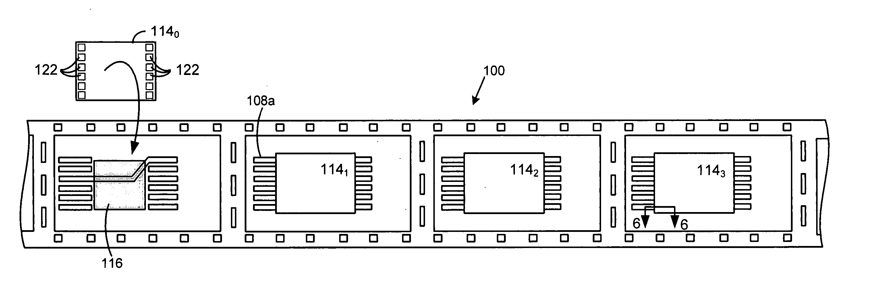
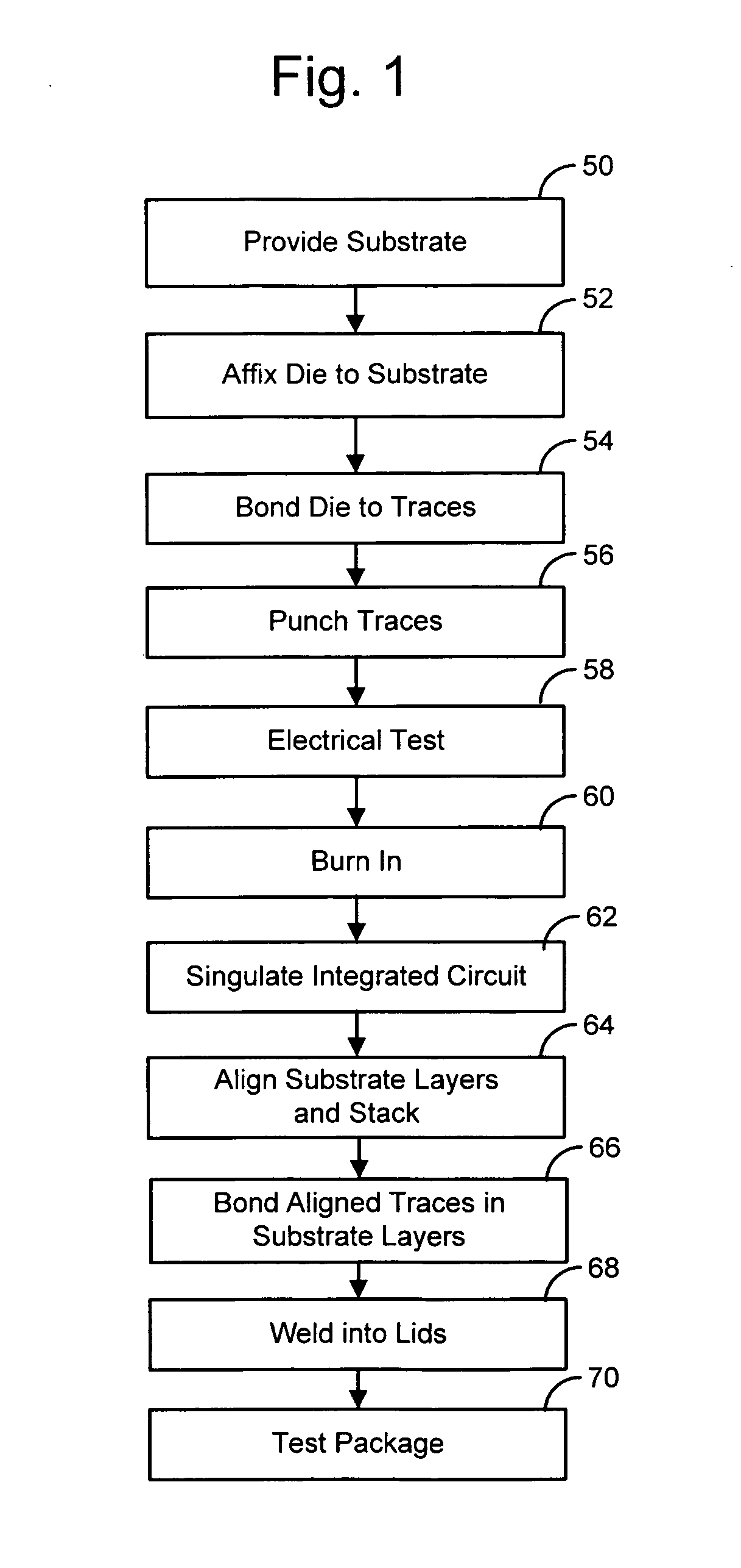
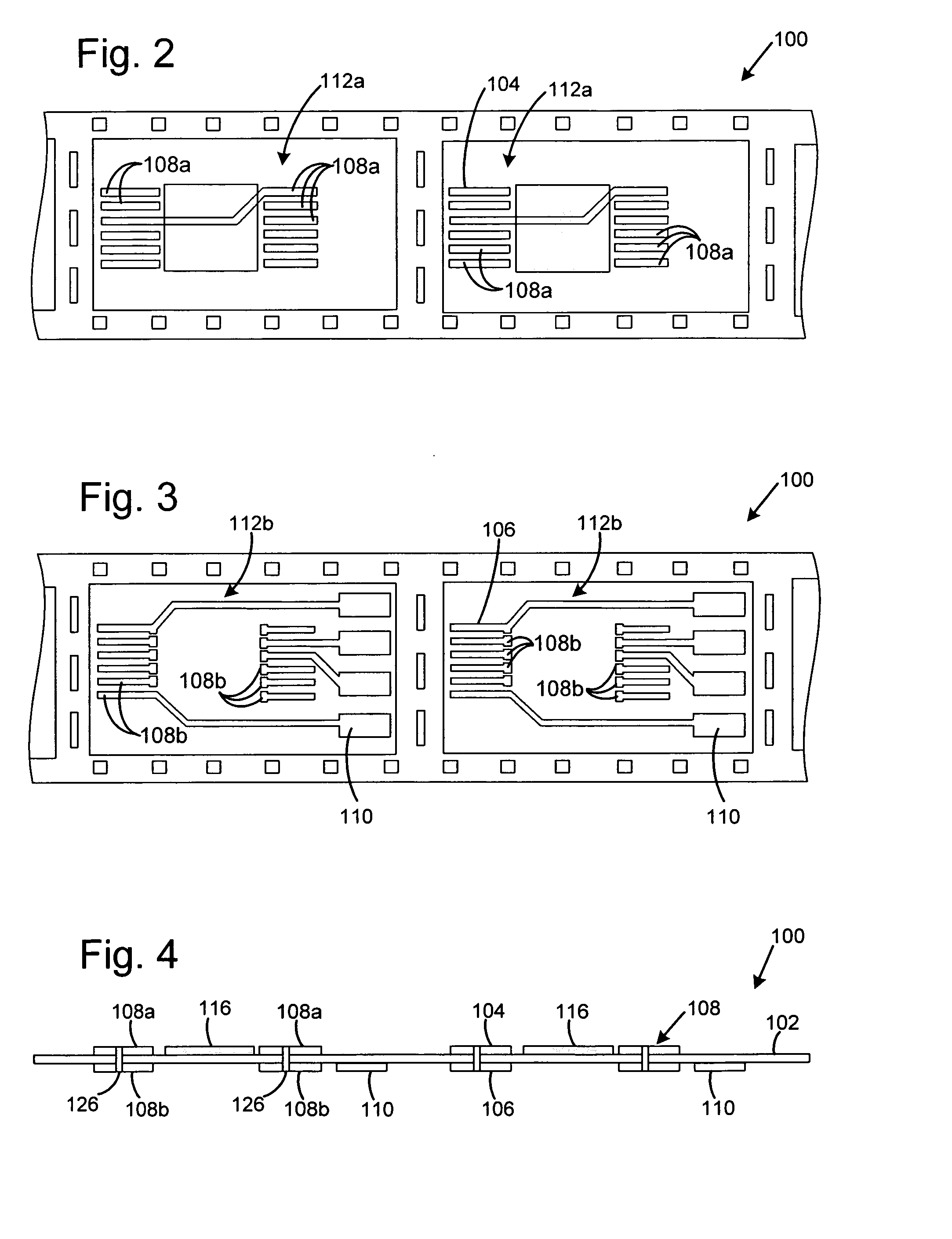
[0025] Embodiments of the invention will now be described with reference to FIGS. 1 through 11 which relate to a semiconductor package including stacked and bonded layers of integrated circuit substrates. It is understood that the present invention may be embodied in many different forms and should not be construed as being limited to the embodiments set forth herein. Rather, these embodiments are provided so that this disclosure will be thorough and complete and will fully convey the invention to those skilled in the art. Indeed, the invention is intended to cover alternatives, modifications and equivalents of these embodiments, which are included within the scope and spirit of the invention as defined by the appended claims. Furthermore, in the following detailed description of the present invention, numerous specific details are set forth in order to provide a thorough understanding of the present invention. However, it will be clear to those of ordinary skill in the art that the...


PUM


Abstract

A semiconductor package is disclosed including a plurality semiconductor die mounted on stacked and bonded layers of substrate, for example polyimide tape used in tape automated bonding processes. The tape may have a plurality of repeating patterns of traces and contact pads formed thereon. The traces each include aligned interconnect pads on the respective top and bottom surfaces of the substrate for bonding the traces of one pattern to the traces of another pattern after the patterns have been singulated from the substrate, aligned and stacked. Semiconductor die such as flash memory and a controller die are mounted on the traces of the respective patterns on the substrate. In order for the controller die to uniquely address a specific flash memory die in the stack, a group of traces on each substrate supporting the memory die are used as address pins and punched in a unique layout relative to the layout of the traces other substrates. By providing each flash memory semiconductor die on a substrate with a unique layout of address traces, each memory die may be selectively addressed by the controller die.

Description

BACKGROUND OF THE INVENTION [0001] 1. Field of the Invention [0002] Embodiments of the present invention relate to a semiconductor package formed of multiple semiconductor die stacked on substrate layers in a three dimensional arrangement. [0003] 2. Description of the Related Art [0004] The strong growth in demand for portable consumer electronics is driving the need for high-capacity storage devices. Non-volatile semiconductor memory devices, such as flash memory storage cards, are becoming widely used to meet the ever-growing demands on digital information storage and exchange. Their portability, versatility and rugged design, along with their high reliability and large capacity, have made such memory devices ideal for use in a wide variety of electronic devices. These devices include for example digital music players, cellular phones, handheld PCs, digital cameras, digital video camcorders, smart phones, car navigation systems and electronic books. [0005] Flash memory storage car...

Claims


Application Information

Patent Timeline
Patent Type & Authority Applications(United States)
IPC IPC(8): H01L23/495
CPCG11C5/02G11C5/04G11C5/143G11C8/12H01L21/485H01L23/5382H01L25/0657H01L2225/06527H01L2225/06579H01L25/50H01L2924/0002H01L2924/00H01L23/12H01L23/48
Inventor YU, CHEEMENLIAO, CHIH-CHINTAKIAR, HEM
Owner SANDISK TECH LLC
Why Eureka
Try Eureka