Implantable microelectronic device and method of manufacture

a microelectronic device and manufacturing method technology, applied in the direction of semiconductor devices, semiconductor/solid-state device details, therapy, etc., can solve the problems of imposing a long life requirement on the manner of hermetic sealing, the contact pads of semiconductor devices cannot be simply left exposed, and the structure is generally more difficult to fabrica

Inactive Publication Date: 2007-05-03
SECOND SIGHT MEDICAL PRODS
View PDF8 Cites 47 Cited by
  • Summary
  • Abstract
  • Description
  • Claims
  • Application Information

AI Technical Summary

Benefits of technology

[0010] In a first aspect, the present invention is directed to an implantable microelectronic device having an electrical contact pad that is made of a non-biocompatible material; a plurality of thin, biocompatible, patterned conductive layers formed over the electrical contact pad, the top surface of the patterned conductive layers defining an electrical contact, and the first conductive layer being in direct contact with the electrical contact pad; a biocompatible electrically insulating material hermetically surrounding the device, the electrically insulating material having an aperture wherein the electrical contact is positioned. Preferably the electrically insulating material is a biocompatible ceramic, such as alumina, and the patterned conductive layers comprise one or more platinum layers formed on one or more titanium layers. The microelectronic device may be an integrated circuit chip, such that the electrical contact pad is aluminum or copper. Preferably, the first patterned conductive layer is larger in its lateral dimensions than the contact pad, such that the layer extends beyond the edge of the contact pad, forming a shoulder.

Problems solved by technology

Many such implantable devices are intended to remain in place over long periods of time, imposing a long life requirement on the manner of hermetic sealing.
Thus, semiconductor device contact pads cannot simply be left exposed by patterning the surrounding alumina layer.
While use of a serpentine structure may overcome this inadequacy, such structures are generally more difficult to fabricate and, in some instances, consume valuable “real estate” on the surface of the device.
Unfortunately, this solution has limited applicability to extremely thin films that can be rendered suitably conductive by ion implantation.

Method used


Image

  • Implantable microelectronic device and method of manufacture
  • Implantable microelectronic device and method of manufacture
  • Implantable microelectronic device and method of manufacture

Examples


Embodiment Construction

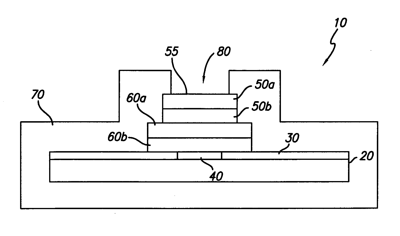
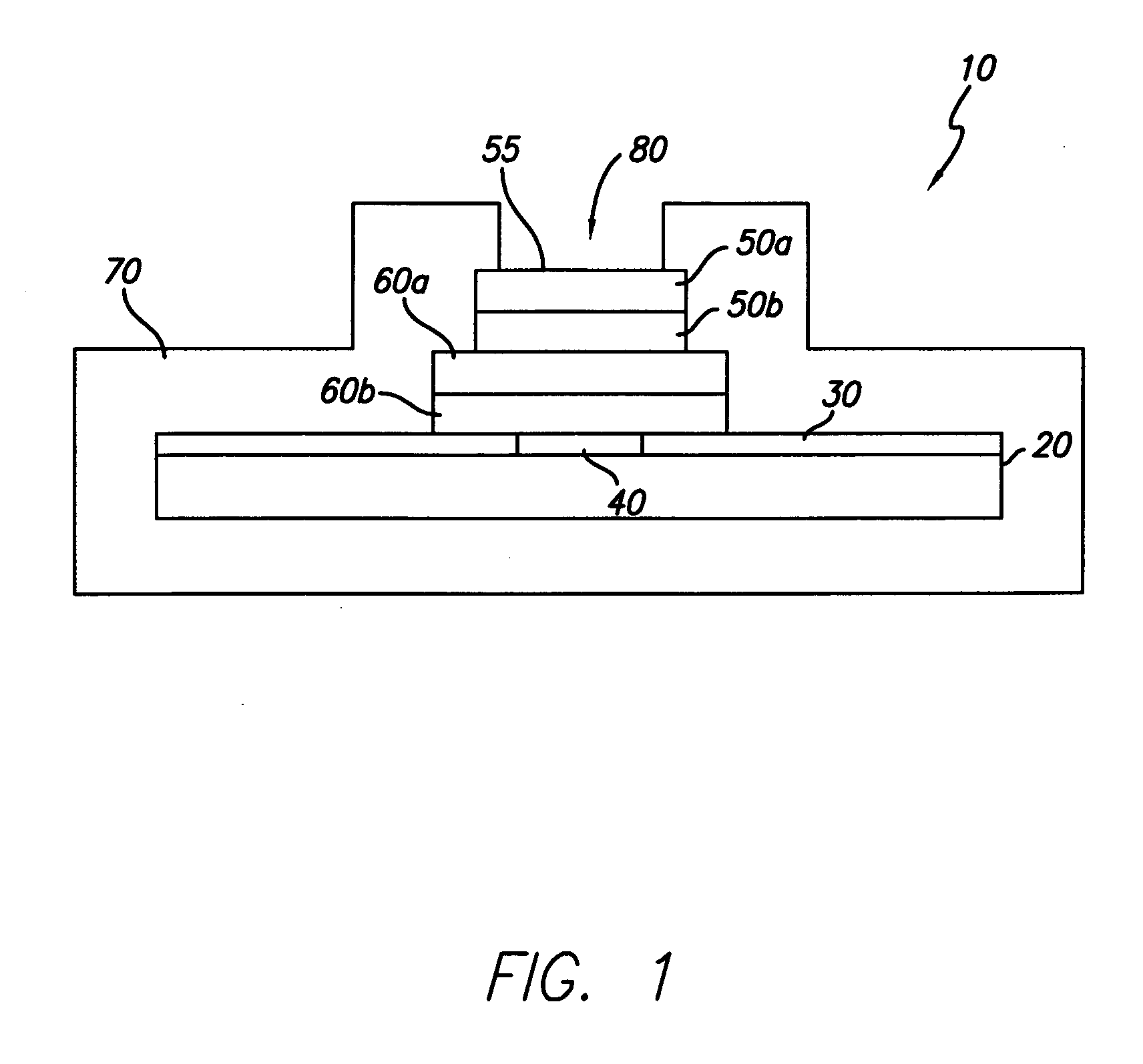
[0024] In general, the present invention is directed to an implantable micro-miniature electronic device, and method of manufacture, with an external electrical contact surface, that has excellent hermetic properties.

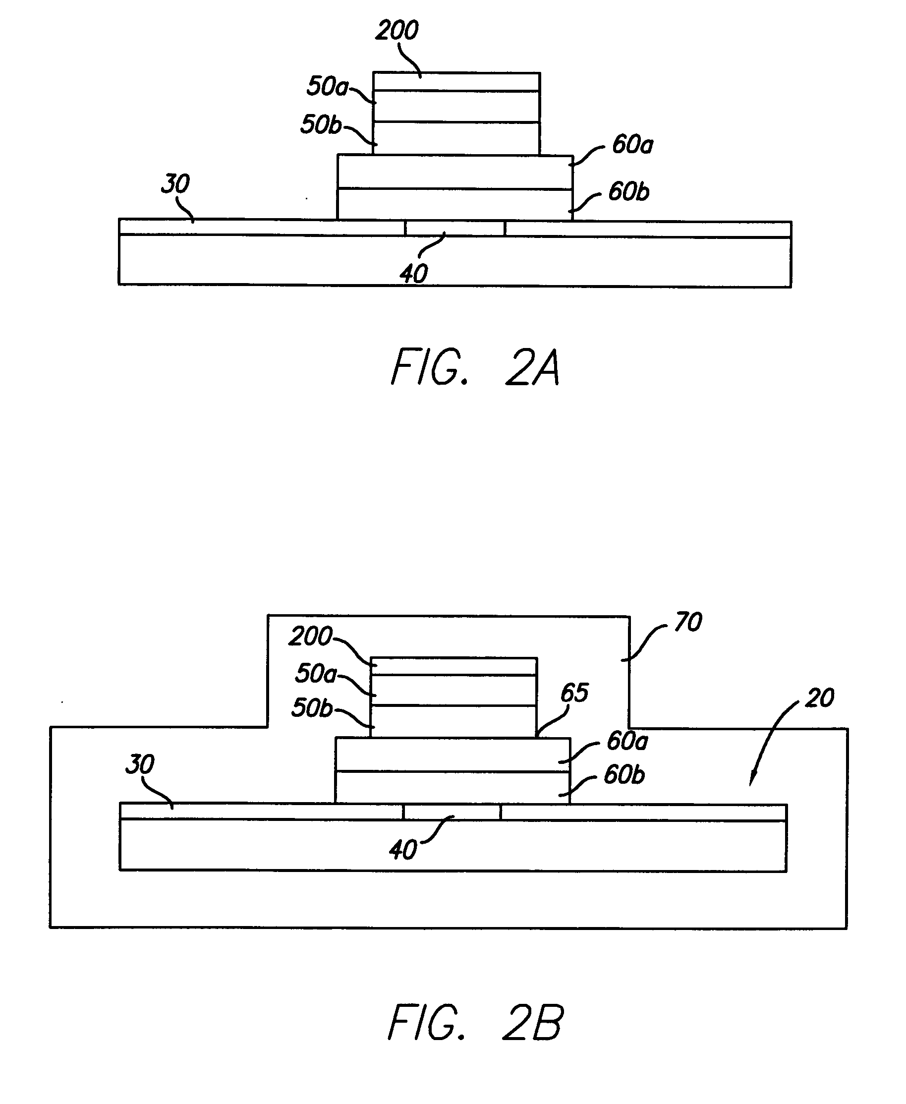
[0025] An exemplary embodiment of an implantable microelectronic device 10 of the present invention is depicted in the simplified, cross-sectional view of FIG. 1. A silicon integrated circuit chip (“IC”) 20 comprises a top electrically insulating (passivation) layer 30 and an electrical contact pad 40 which extends through layer 30 to the surface of IC 20. While the exemplary embodiment of the invention is described in conjunction with IC 20, the invention is also useful with other types of microelectronic devices, whether or not they are fabricated on silicon, which require a hermetic electrical connection. Therefore, the present invention should not be viewed as restricted to use with IC chips.

[0026] While only one contact pad 40 is shown in FIG. 1, those skilled in...


PUM


Abstract

An implantable hermetically sealed microelectronic device, and method of manufacture are disclosed. The microelectronic device of the present invention is hermetically encased in a insulator, such as alumina formed by ion bean assisted deposition (“IBAD”), with a stack of biocompatible conductive layers extending from a contact pad on the device to an aperture in the hermetic layer. In a preferred embodiment, one or more patterned titanium layers are formed over the device contact pad, and one or more platinum layers are formed over the titanium layers, such that the top surface of the upper platinum layer defines an external, biocompatible electrical contact for the device. Preferably, the bottom conductive layer is larger than the contact pad on the device, and a layer in the stack defines a shoulder.

Description

CROSS-REFERENCE TO RELATED APPLICATIONS [0001] This application claims priority of Provisional Patent Application No. 60 / 732,884, “Implantable Microelectronic Device and Method of Manufacture,” filed Nov. 02, 2005, the disclosure of which is incorporated herein by reference.FEDERALLY SPONSORED RESEARCH [0002] This invention was made with governmental support under grant No. R24EY12893-01, awarded by the National Institutes of Health. The federal government has certain rights in this invention.FIELD OF THE INVENTION [0003] The present invention is related to implantable medical devices, and is particularly related to implantable microelectronic devices. BACKGROUND OF THE INVENTION [0004] Biocompatibility is a critical concern for medical devices that are designed to be implanted in vivo. Biocompatibility is necessary to avoid adverse reactions in the subject, and to avoid device failure as a result of exposure to the corrosive saline body fluids and other substances in the tissue sur...

Claims


Application Information

Patent Timeline
Patent Type & Authority Applications(United States)
IPC IPC(8): H01L23/20H01L23/10H01L23/043H01L21/00
CPCA61N1/375H01L2224/0401H01L23/291H01L23/3107H01L24/12H01L24/85H01L2224/0345H01L2224/0347H01L2224/05083H01L2224/05124H01L2224/05147H01L2224/05164H01L2224/05166H01L2224/05187H01L2224/05624H01L2224/05647H01L2224/13099H01L2224/13164H01L2224/13169H01L2924/01005H01L2924/01013H01L2924/01014H01L2924/01015H01L2924/01018H01L2924/01022H01L2924/01027H01L2924/01028H01L2924/01029H01L2924/01046H01L2924/01047H01L2924/01077H01L2924/01078H01L2924/01079H01L2924/04941H01L2924/14H01L2924/1433A61N1/3754H01L2924/00014H01L2924/10253H01L2224/85H01L2924/01041H01L2924/01033H01L2924/01024H01L2924/01019H01L2924/01006H01L24/05H01L24/03H01L2924/04953H01L2924/00H01L2224/48H01L2924/351H01L2924/12042H01L2224/45015H01L2924/207H01L2224/45099
Inventor GREENBERG, ROBERT J.TALBOT, NEIL HAMILTONNEYSMITH, JORDAN MATTHEWOK, JERRYJIANG, HONGGANG
Owner SECOND SIGHT MEDICAL PRODS
Why Eureka
Try Eureka