Optical signal jitter reduction via electrical equalization in optical transmission systems

a technology of optical transmission system and electrical equalization, applied in the field of optical transmission system, can solve the problems of increasing cost, increasing jitter on the output optical signal, adding cost, etc., and achieve the effect of reducing electrical and optical material costs and improving jitter performan

Inactive Publication Date: 2007-05-03
AVAGO TECH WIRELESS IP SINGAPORE PTE
View PDF5 Cites 9 Cited by
  • Summary
  • Abstract
  • Description
  • Claims
  • Application Information

AI Technical Summary

Benefits of technology

[0010] The illustrative embodiment provides a number of significant advantages over the conventional techniques previously described. For example, as indicated above, applying equalization to the electrical signal can compensate for characteristics of both the interconnect channel and the electrical-to-optical converter. As a result, such equalization can reduce electrical and optical material costs and relax physical placement constraints for a given level of jitter performance, or it can improve jitter performance for a given material cost and physical placement constraint.

Problems solved by technology

A problem associated with such an arrangement is that the jitter on the output optical signal can increase due to effects of the interconnect channel and properties of the electrical-to-optical converter.
Unfortunately, maintaining a high quality interconnect channel in an optical transmission system either adds cost by requiring more costly high performance materials, or it constrains the physical configuration and distance over which system components can be interconnected leading to lower density solutions or less flexible physical designs.

Method used


Image

  • Optical signal jitter reduction via electrical equalization in optical transmission systems
  • Optical signal jitter reduction via electrical equalization in optical transmission systems
  • Optical signal jitter reduction via electrical equalization in optical transmission systems

Examples


Embodiment Construction

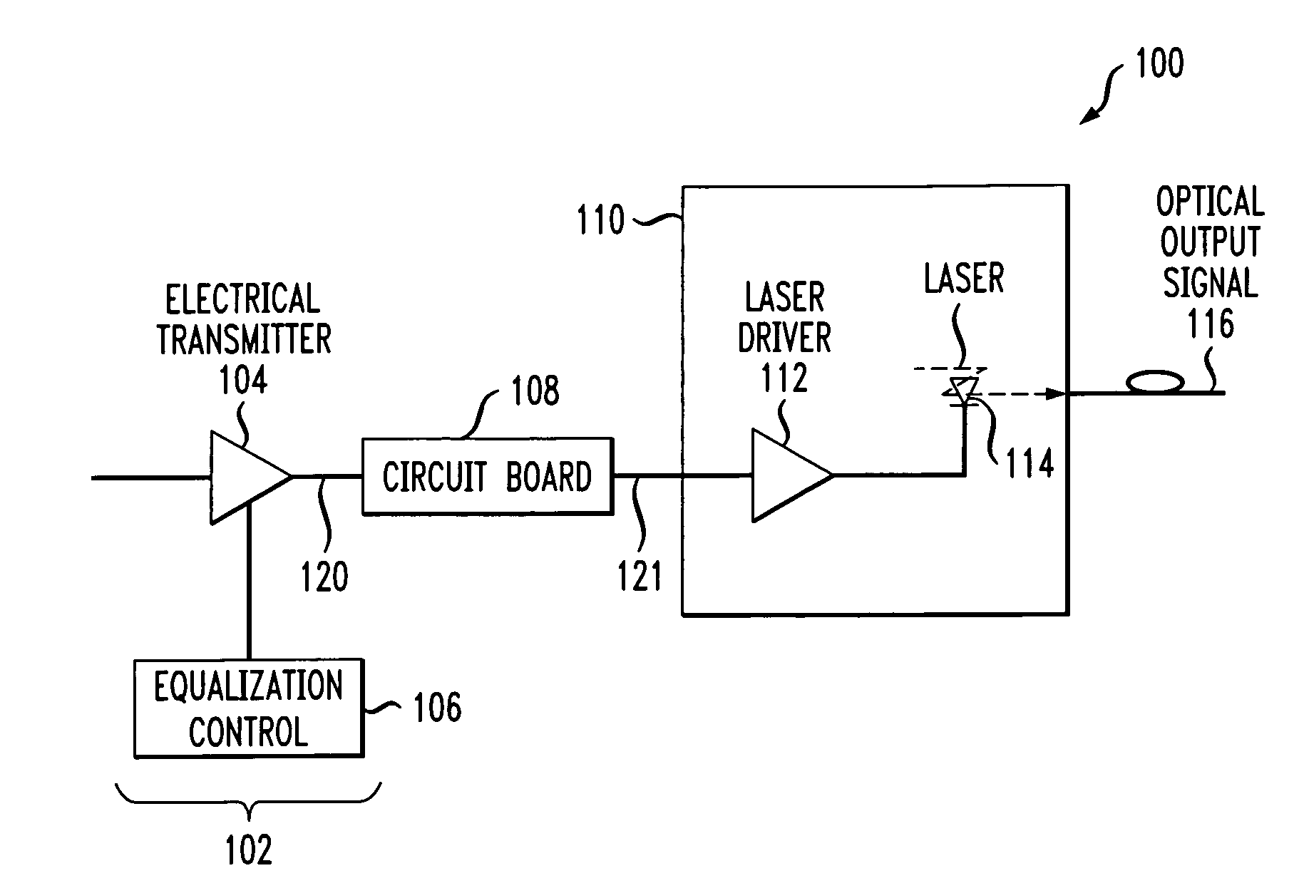
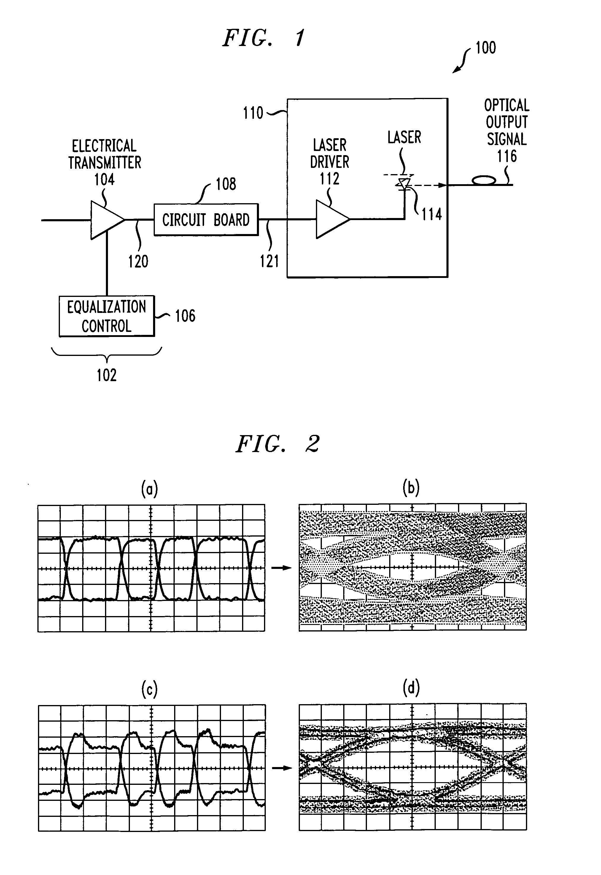
[0017] The invention will be illustrated herein in conjunction with exemplary communication systems comprising one or more optical transmission systems. It should be understood, however, that the invention is more generally applicable to any optical transmission system involving electrical-to-optical signal conversion in which it is desirable to provide enhanced control of output optical signal jitter. The term “jitter” as used herein is intended to be construed broadly so as to encompass, by way of example, not only actual jitter measurements but other related characterizations of jitter, including those based on signal integrity measures such as signal rise and fall times, transmit eye openings, etc.

[0018]FIG. 1 shows an optical transmission system 100 in accordance with an illustrative embodiment of the invention. The system 100 comprises an electrical source 102 adapted to provide an electrical signal at an output thereof. The electrical source 102 in this embodiment further co...


PUM


Abstract

An optical transmission system comprises an electrical source and an electrical-to-optical converter. The electrical source is adapted to provide an electrical signal at an output thereof. The electrical-to-optical converter has an input coupled to the output of the electrical source and is operative to convert the electrical signal to a corresponding output optical signal. The electrical source comprises a pre-emphasis circuit or other electrical signal equalization circuitry configurable to control a waveform of the electrical signal so as to produce a desired level of jitter in the output optical signal.

Description

FIELD OF THE INVENTION [0001] The present invention relates generally to communication systems, and more particularly to optical transmission systems which convert electrical signals from one or more electrical sources to optical signals for transmission. BACKGROUND OF THE INVENTION [0002] In a typical optical transmission system, an electrical source drives an electrical-to-optical converter through a band-limited interconnect channel. For example, an electrical transmitter may be coupled to an electrical-to-optical converter via one or more traces of a circuit board formed of FR4 or another type of material. [0003] A problem associated with such an arrangement is that the jitter on the output optical signal can increase due to effects of the interconnect channel and properties of the electrical-to-optical converter. Optical transmission systems designed to operate in accordance with well-known optical communications standards, such as the synchronous optical network (SONET) and sy...

Claims


Application Information

Patent Timeline
Patent Type & Authority Applications(United States)
IPC IPC(8): H04B10/04H04B10/43
CPCH04B10/504H04B10/58
Inventor SCOGGINS, JOHN E.SIULINSKI, JAMES A.SNOWDON, KENNETH P.
Owner AVAGO TECH WIRELESS IP SINGAPORE PTE
Why Eureka
Try Eureka