Semiconductor-integrated circuit utilizing magnetoresistive effect elements

Inactive Publication Date: 2007-05-10
SONY CORP
View PDF8 Cites 122 Cited by
  • Summary
  • Abstract
  • Description
  • Claims
  • Application Information

AI Technical Summary

Benefits of technology

[0012] According to a fourth aspect of the present invention, there is provided a semiconductor integrated circuit device including a semiconductor substrate, a plurality of circuit selection switching elements formed on said semiconductor substrate, a first insulating film formed on said semiconductor substrate, a power supply line formed at the first insulating film, and a first circuit forming layer having a second insulating film formed at said first insulating film and having a first interconnect used as a control line formed inside it, a magnetoresistance effect element formed on the surface of the second insulating film, and a second interconnect formed on the magnetoresistance effect element, wherein a via hole in which a conductive member is filled is formed in said second insulating film close to said magnetoresistance effect element, said power supply line is connected to one end of said conductive member, said second interconnect is connected to the other end of said conductive member, a drive input terminal of said circuit switching element is connected to a terminal for applying a circuit configuration instruction signal input from the outside of the semicondu

Problems solved by technology

However, the conventional integrated circuit devices having logic elements and memory elements mounted together suffer from the following disadvantages.
First, in the improvement of the degree of integration, since the structure is restricted to a two-dimensional plane, the area in the two-dimensional plane

Method used


Image

  • Semiconductor-integrated circuit utilizing magnetoresistive effect elements
  • Semiconductor-integrated circuit utilizing magnetoresistive effect elements
  • Semiconductor-integrated circuit utilizing magnetoresistive effect elements

Examples


Embodiment Construction

[0045] An explanation will be given below of embodiments of the architectures of an integrated circuit and an integrated circuit device of the present invention.

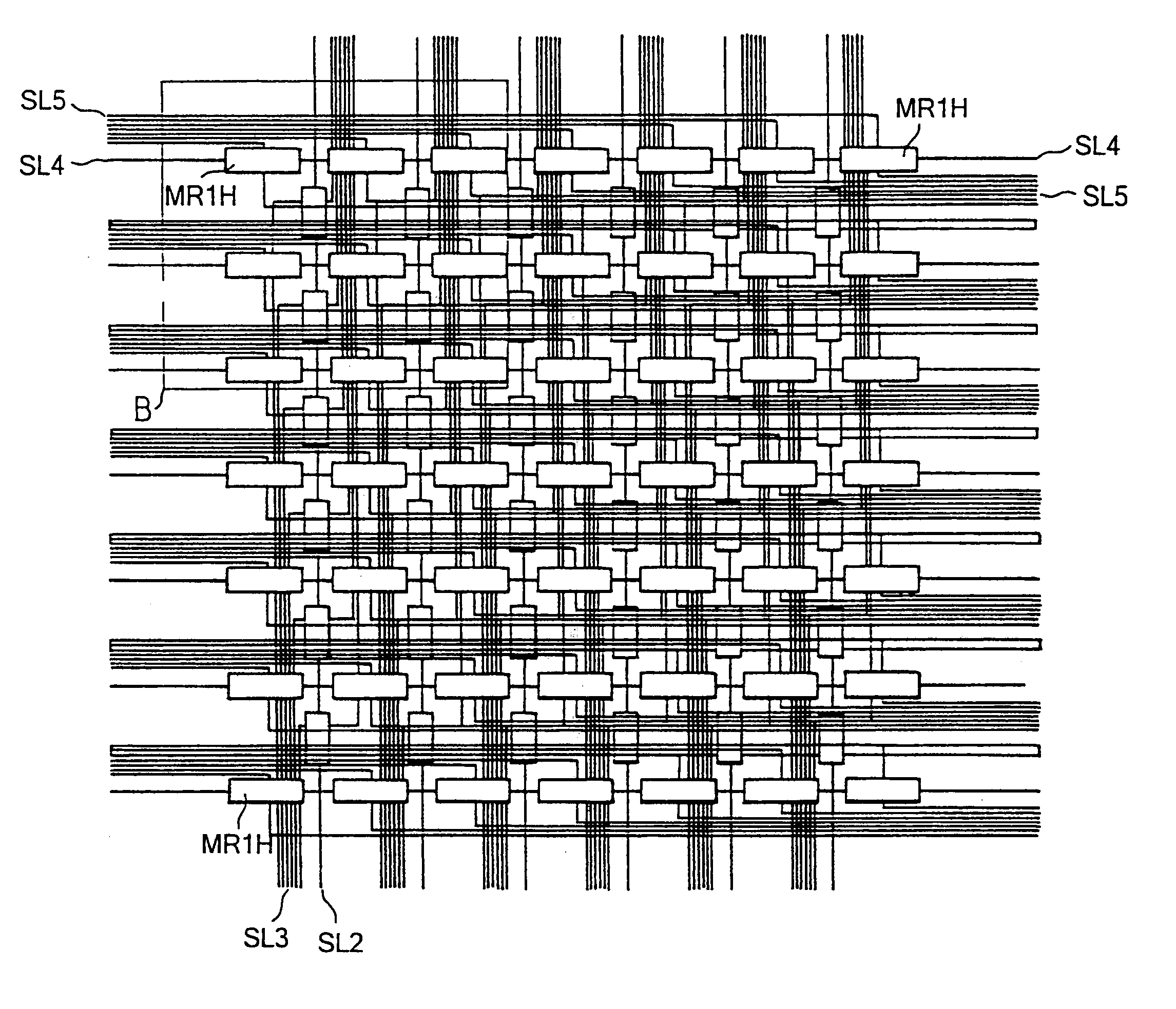
[0046] An example of an integrated circuit device of the present invention will be explained below. The integrated circuit device of the present invention is an integrated circuit device configured by a plurality of elements or a plurality of integrated circuits which applies either of the methods of operation of the integrated circuit devices of the present invention explained before to repeatedly generate spaces acting as any circuit functions or release the addresses of circuit functions so as to divide in time and divide in space the functions of the elements or the integrated circuits.

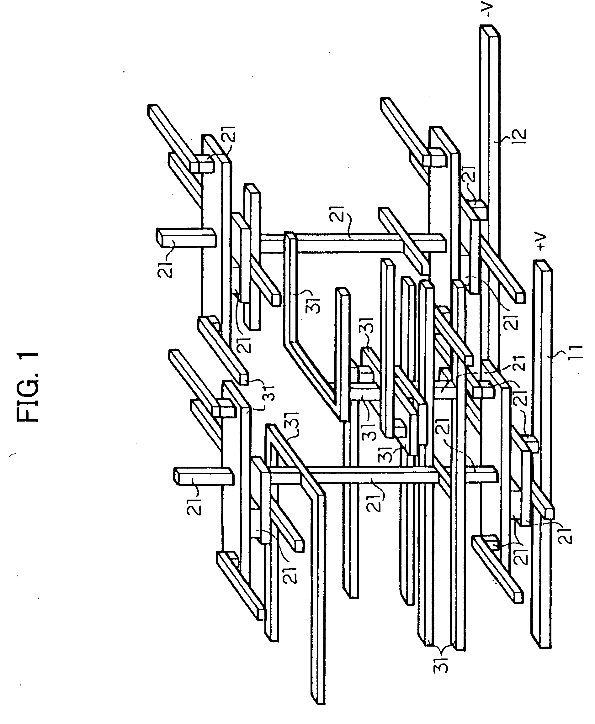
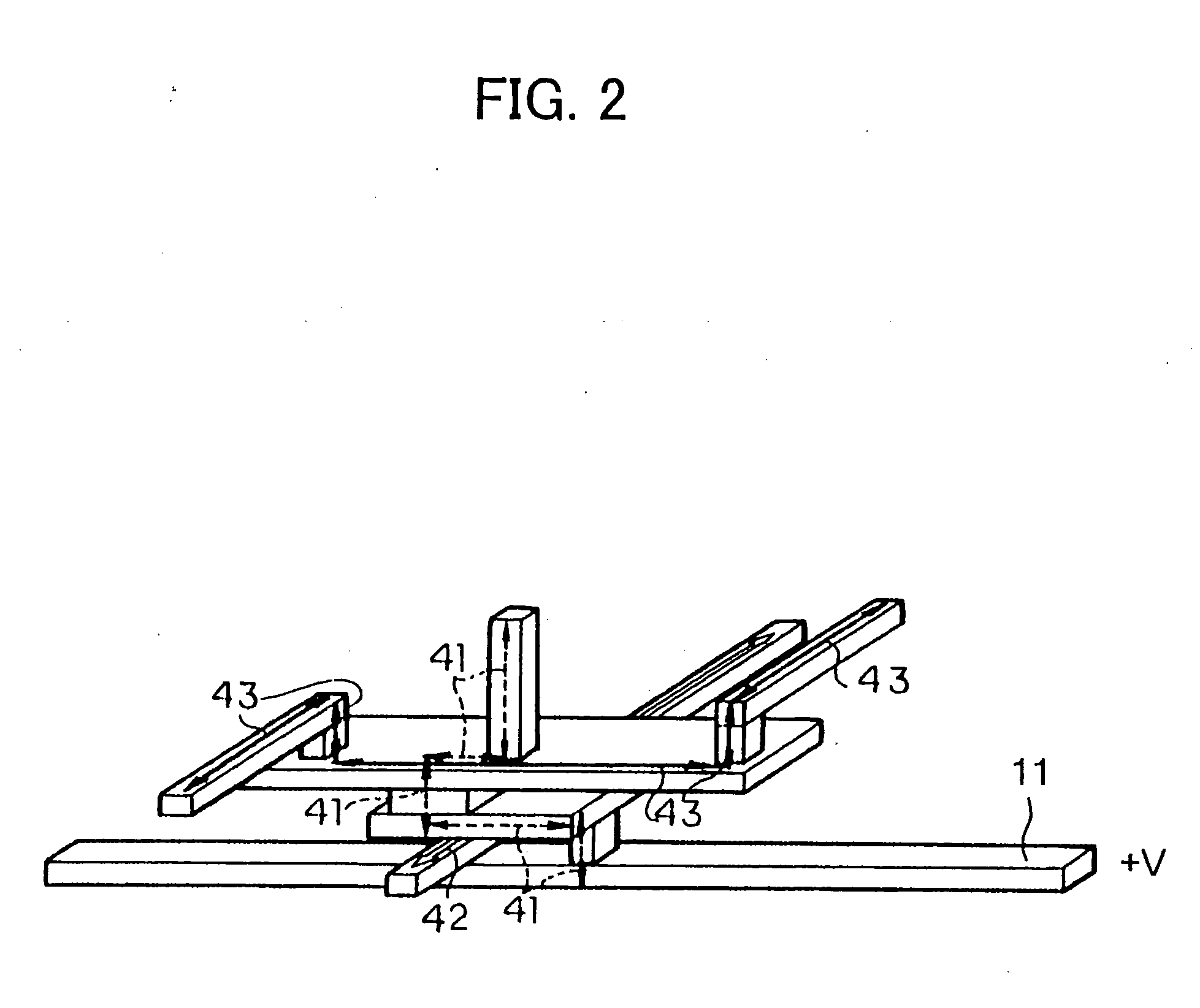
[0047] In general, an integrated circuit device providing a plurality of circuit functions, for example, as illustrated in FIGS. 34A to 34C, is realized by using as switching function elements either or both of magnetoresistance effect e...


PUM


Abstract

A semiconductor integrated circuit device able to configure a desired circuit in accordance with a circuit configuration instruction signal given from the outside and able to operate the configured circuit is provided. The semiconductor integrated circuit device has a plurality of circuit elements, a plurality of connection elements each of which becomes a conductive state or a nonconductive state, interconnects for supplying control signals for placing the connection elements in the conductive state or the nonconductive state, and a plurality of circuit selection switching elements, wherein said circuit selection switching elements are driven in response to the circuit configuration instruction signal, control signals are output from the circuit selection switching elements, and the desired circuit is configured by combining the circuit elements via said connection elements which become the conductive state or the nonconductive state in accordance with the control signals. As the connection elements, preferably use is made of magnetoresistance effect elements or resistance control elements which become the conductive state or the nonconductive state in accordance with application of a magnetic field. As the circuit elements, use can be made of magnetoresistance effect elements or resistance control elements.

Description

TECHNICAL FIELD [0001] The present invention relates to an integrated circuit device configured by a logic circuit and a memory circuit and changing in function every certain time interval and a method of configuration and a method of production of an integrated circuit device, more particularly relates to an architecture of an integrated circuit device for dynamically securing an address space to be used for obtaining a targeted logic function and memory function in elements or a set of integrated circuits having addresses allocated thereto and performing instruction processing or action as a memory, a method of configuration of an integrated circuit device, and a method of production of an integrated circuit device. BACKGROUND ART [0002] In image processing, audio processing, mobile terminal, or other information communication apparatuses or processing apparatuses, an integrated circuit devices configured by logic elements and memory elements are being required to offer higher per...

Claims


Application Information

Patent Timeline
IPC IPC(8): H03K19/173H01L21/335H01L21/82H01L21/8232H01L23/48H01L23/52H01L27/02H01L27/10H01L27/105H01L27/108H01L27/146H01L27/22H01L27/24H01L43/08H03K19/177
CPCH01L27/0207H01L27/105H01L27/10897H01L27/14601H01L27/228H01L2924/0002H01L27/24H01L2924/00H10B63/30H10B61/22H10B12/50H01L21/18H01L23/52H01L23/48H01L21/8232H10B63/00
Inventor SUGAWARA, MINORUMOTOYOSHI, MAKOTO
Owner SONY CORP
Why Eureka
Try Eureka