Integrated circuit package system with arched pedestal

a technology of integrated circuit and pedestal, which is applied in the field of integrated circuit package systems, can solve the problems of reducing thermal performance, high manufacturing cost of stacked dies, and adversely affecting the performance of packages

Active Publication Date: 2007-05-17
STATS CHIPPAC LTD
View PDF6 Cites 15 Cited by
  • Summary
  • Abstract
  • Description
  • Claims
  • Application Information

AI Technical Summary

Problems solved by technology

Unfortunately, the stacking adversely affects the performance of the package because of decreased thermal performance due to the inability to remove heat through the organic adhesive and / or inorganic spacers.
Further, such stacked dies have a high manufacturing cost.
Another approach is to put more integrated circuit dies side-by-side in a single package but this results in packages taking up large areas on the printed circuit boards.
Each attempt to reduce the size of the integrated circuit package tends to create additional problems with cost, heat transfer, and electrical performance.
Solutions to these problems have been long sought but prior developments have not taught or suggested any solutions and, thus, solutions to these problems have long eluded those skilled in the art.

Method used


Image

  • Integrated circuit package system with arched pedestal
  • Integrated circuit package system with arched pedestal
  • Integrated circuit package system with arched pedestal

Examples


Embodiment Construction

[0025] In the following description, numerous specific details are given to provide a thorough understanding of the invention. However, it will be apparent that the invention may be practiced without these specific details. In order to avoid obscuring the present invention, some well-known circuits, and process steps are not disclosed in detail.

[0026] Likewise, the drawings showing embodiments of the apparatus / device are semi-diagrammatic and not to scale and, particularly, some of the dimensions are for the clarity of presentation and are shown greatly exaggerated in the drawing FIGs. Similarly, although the sectional views in the drawings for ease of description show the invention with surfaces as oriented downward, this arrangement in the FIGs. is arbitrary and is not intended to suggest that invention should necessarily be in a downward direction. Generally, the device can be operated in any orientation. In addition, the same numbers are used in all the drawing FIGs. to relate ...


PUM


Abstract

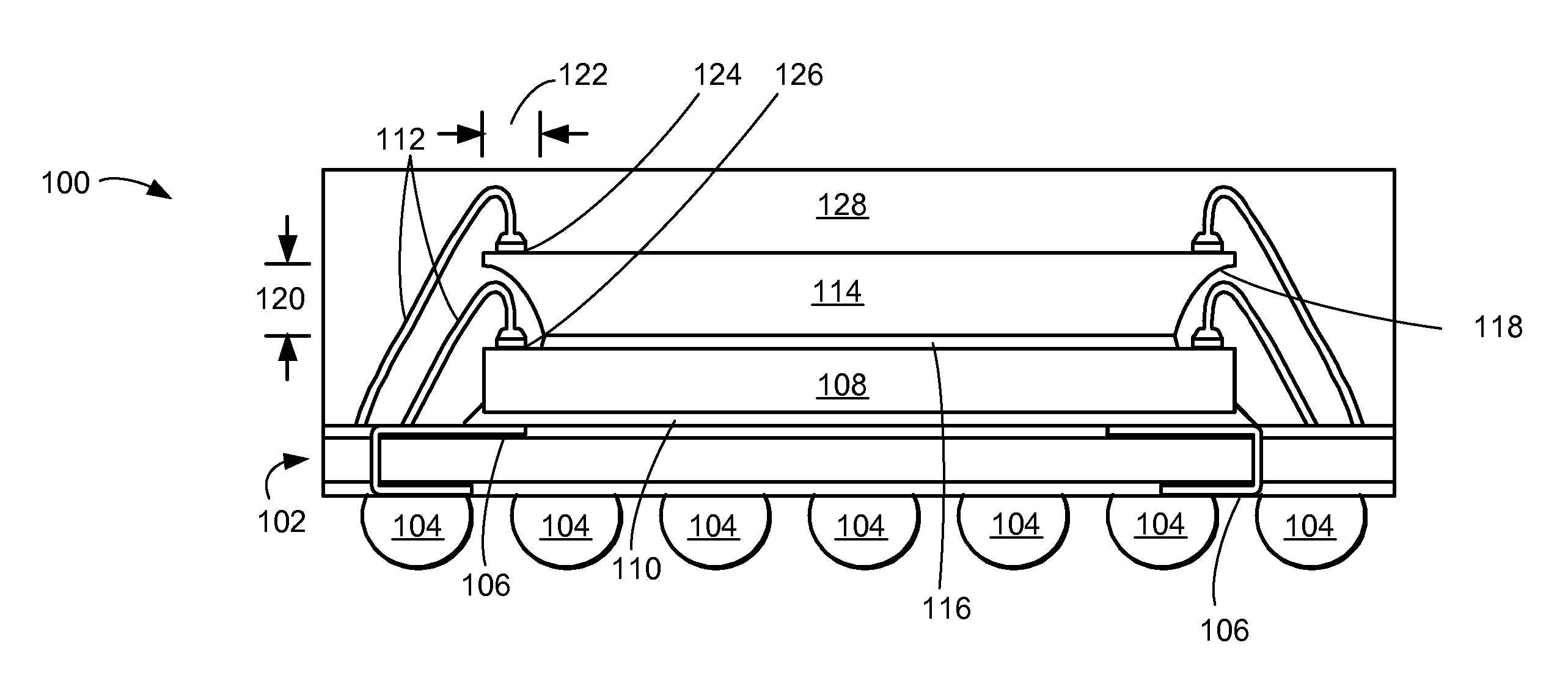
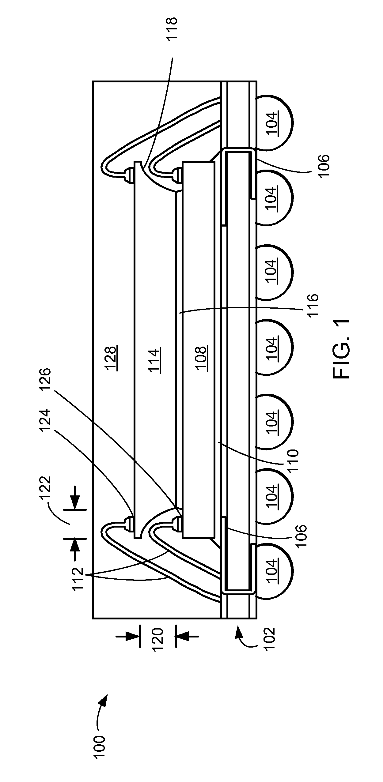
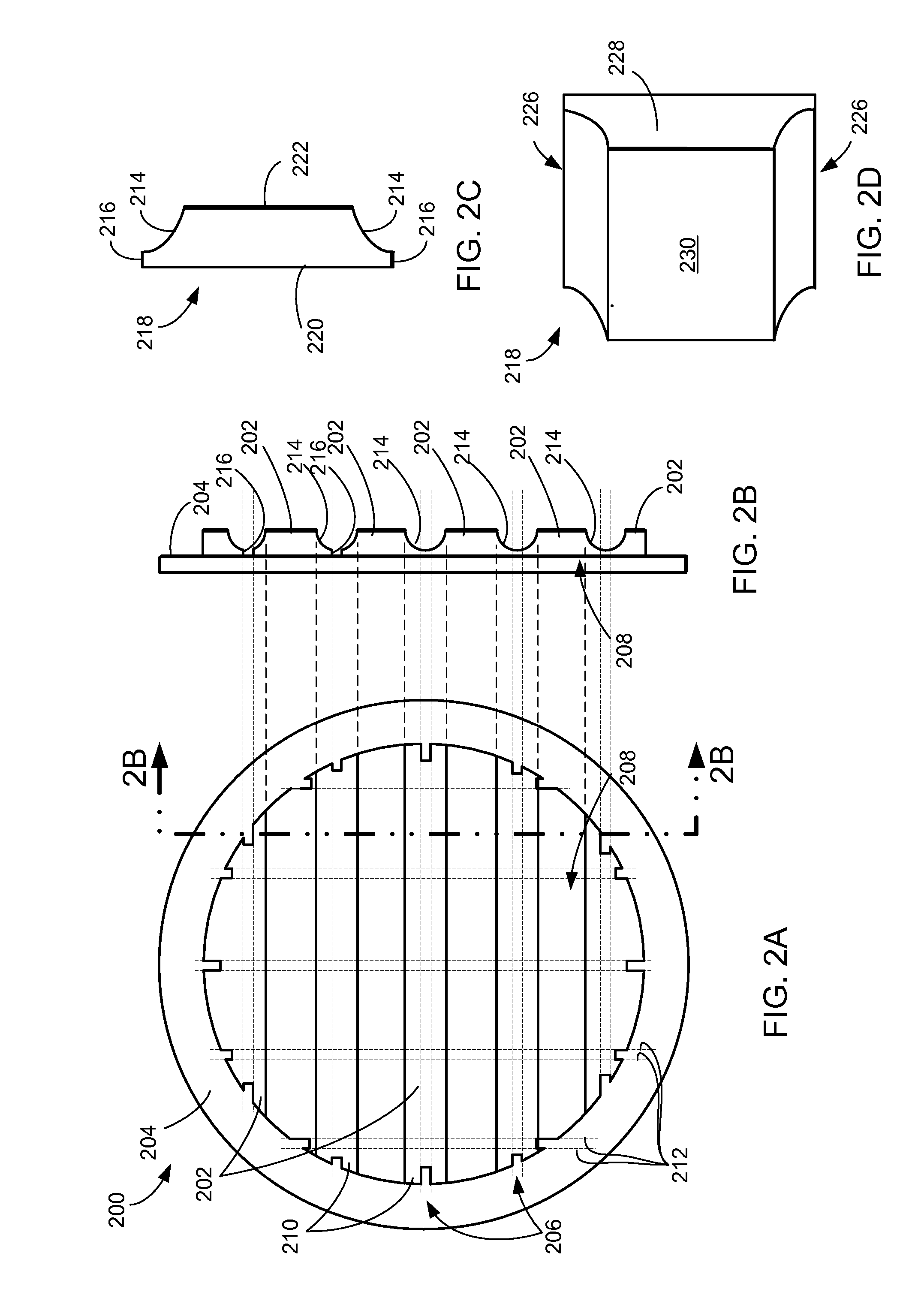
An integrated circuit package system includes an arched pedestal integrated circuit die including an active surface, a die mounting surface, a pedestal portion including an arch intersecting the die mounting surface and having an arch height, and the arch under a portion of the active surface and having an arch width less than the arch height.

Description

CROSS-REFERENCE TO RELATED APPLICATION(S) [0001] This application claims the benefit of U.S. Provisional Patent Application Ser. No. 60 / 595,850 filed Aug. 10, 2005.TECHNICAL FIELD [0002] The present invention relates generally to integrated circuit packages, and more particularly to a system for a package for stacked integrated circuits. BACKGROUND ART [0003] In the electronics industry, as products such as cell phones and camcorders become smaller and smaller, increased miniaturization of integrated circuit (IC) packages has become more and more critical. At the same time, higher performance and lower cost have become essential for new products. [0004] Usually, many individual integrated circuit devices are constructed on the same wafer and groups of integrated circuit devices are separated into individual integrated circuit die. [0005] In order to interface an integrated circuit die with other circuitry, it is common to mount it on a leadframe or on a multi-chip module substrate t...

Claims


Application Information

Patent Timeline
Patent Type & Authority Applications(United States)
IPC IPC(8): H01L23/52
CPCH01L25/0657H01L25/50H01L2224/32145H01L2224/48091H01L2224/48227H01L2224/48465H01L2224/73265H01L2225/0651H01L2225/06555H01L2225/06586H01L2924/01079H01L2924/10158H01L2924/15311H01L2924/00014H01L2924/00H01L2224/45124H01L2224/32225H01L2924/00012H01L24/73H01L2924/14
Inventor PARK, SOO-SAN
Owner STATS CHIPPAC LTD
Why Eureka
Try Eureka