Alignment mark with improved resistance to dicing induced cracking and delamination in the scribe region

a technology of alignment marks and which is applied in the direction of semiconductor devices, semiconductor/solid-state device details, electrical apparatus, etc., can solve the problems of failure of semiconductor chips, weak points of electrical interconnects, and little effort to control crack propagation or delamination at alignment structures, so as to achieve maximum surface area exposure

Inactive Publication Date: 2007-05-17
IBM CORP
View PDF5 Cites 11 Cited by
  • Summary
  • Abstract
  • Description
  • Claims
  • Application Information

AI Technical Summary

Benefits of technology

[0017] In a second aspect, the present invention is directed to an alignment mark for resisting dicing induced cracks and delamination on a semiconductor wafer during wafer processing, comprising: a cross-shaped structure centered about the alignment mark for guiding a dicing blade; a plurality of shaped connecting elements having at least two different sizes, the connecting elements arranged about the alignment mark periphery in an alternating pattern ...

Problems solved by technology

These cracks can cause electrical openings or shorts, and ultimately cause failure of the semiconductor chip.
If the delamination or crack reaches an electrical interconnect, the forces within the die that caused the delamination or crack propagation act upon the electrical interconnect causing the electrical interconnect to rip apart at its weak points.
However, th...

Method used


Image

  • Alignment mark with improved resistance to dicing induced cracking and delamination in the scribe region
  • Alignment mark with improved resistance to dicing induced cracking and delamination in the scribe region
  • Alignment mark with improved resistance to dicing induced cracking and delamination in the scribe region

Examples


Embodiment Construction

)

[0024] In describing the preferred embodiment of the present invention, reference will be made herein to FIGS. 1-5 of the drawings in which like numerals refer to like features of the invention.

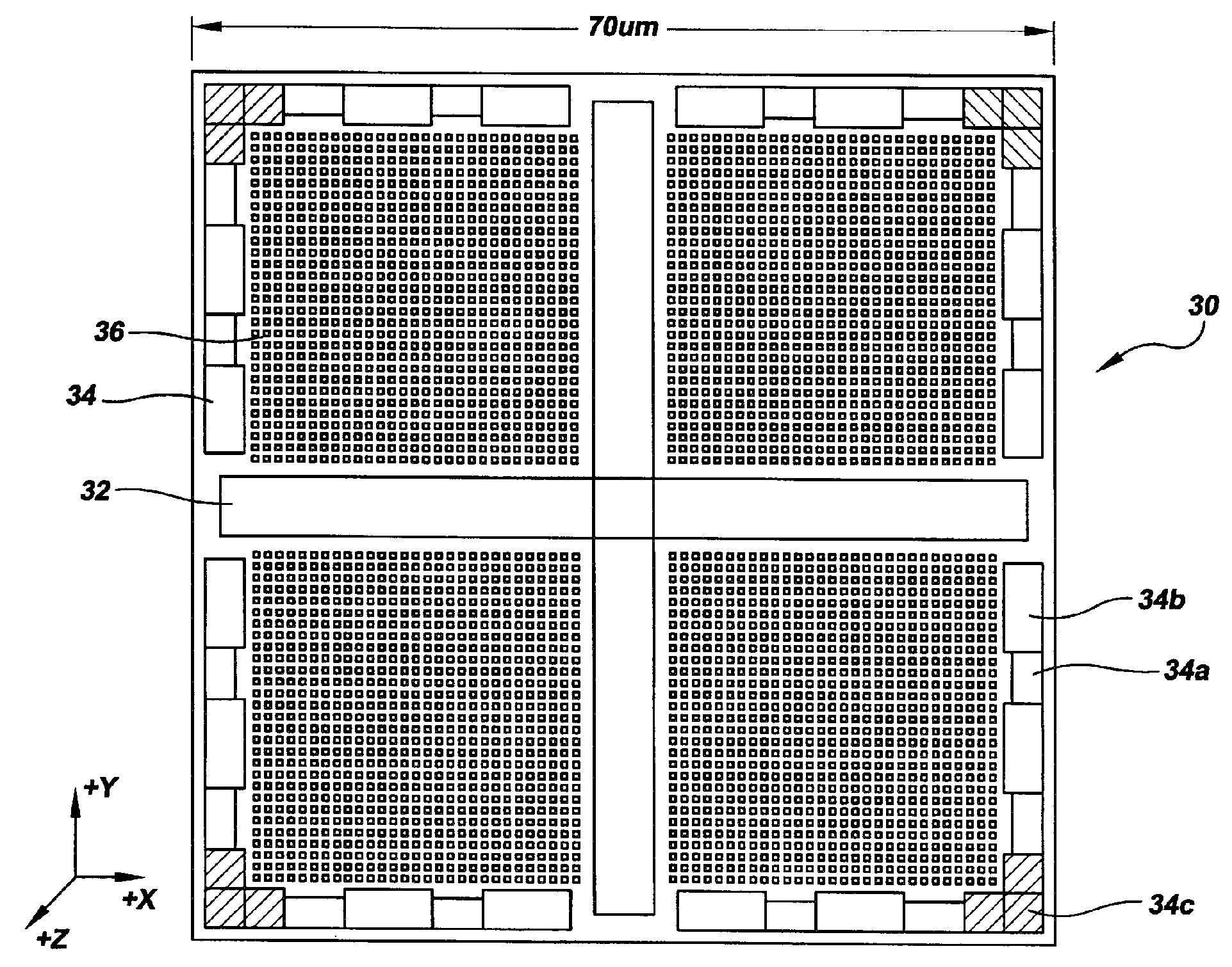
[0025] Stacked via fills of a finite width along a chip edge can prevent the chip from the cracking and delaminating that will ultimately occur during dicing. Preferably, the stacked via fills connect from the bottom of the wafer to the topmost oxide layer, and are either electrically active or dummy vias, but nonetheless, yield a strong structure to protect the weak dielectrics around them.

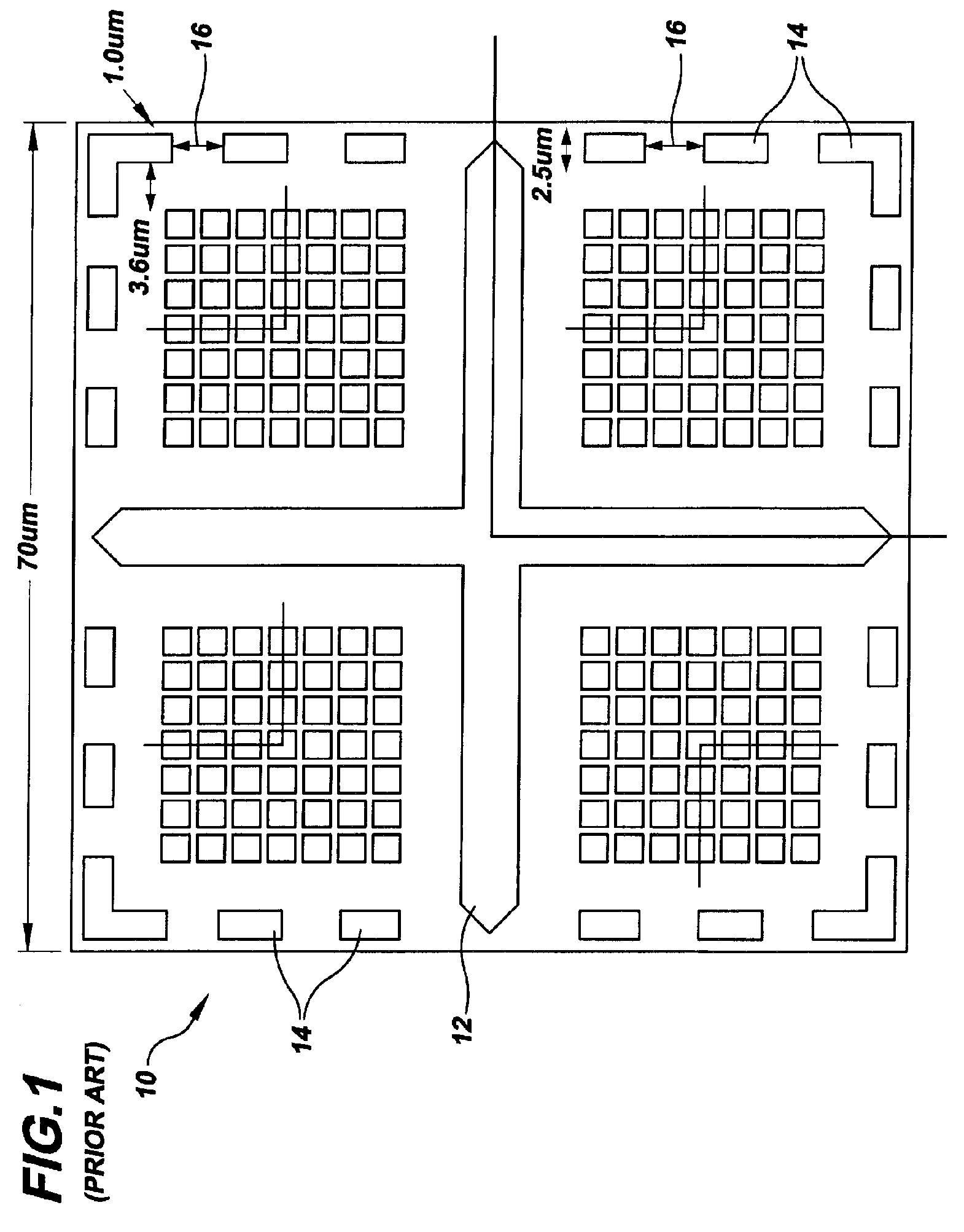
[0026]FIG. 1 depicts a schematic of an alignment mark 10 of the prior art having a cross-shaped structure 12 for dicing blade alignment, and individual surface structures 14 about the periphery. The alignment mark 10 is typically about 70 microns in width, with individual surface structures 14 about the periphery measuring approximately 2.5 microns in width. Surface structures 14 are spaced apart with g...


PUM


Abstract

A robust alignment mark used in semiconductor processing to help deter the expansion of cracks and delamination caused by the cutting of a dicing blade. A cross-shaped structure is used as a line site for alignment of the dicing blade. A plurality of rectangular elements is situated about the periphery of the alignment mark and populated with via bar structures that are interconnected at each level of the wafer, and laid in a serpentine fashion throughout each element to expose more of the via bar structure surface area to propagating cracks. The rectangular elements are formed of different sizes to expose more surface area to propagating cracks. A plurality of square, metal-level structures is formed in the area between the cross-shaped structure and the peripherally placed, rectangular elements.

Description

BACKGROUND OF THE INVENTION [0001] 1. Field of the Invention [0002] This invention relates to structures for preventing cracks from propagating during dicing. More particularly, it relates to resisting dicing induced cracking and delamination on semiconductor wafers. Even more particularly, it relates to patterned structures embedded within the alignment features on a semiconductor wafer that reduce or prevent damage to the integrated circuit by the dicing blade during cutting. [0003] 2. Description of Related Art [0004] Delamination cracks caused by dicing can propagate across an integrated circuit chip inwards from the edge to active regions. These cracks can cause electrical openings or shorts, and ultimately cause failure of the semiconductor chip. The delamination typically allows moisture and other impurities to penetrate in the semiconductor wafer. Typically, the delamination induced by dicing is due, in part, to reduced adhesion or reduced mechanical strength materials that ...

Claims


Application Information

Patent Timeline
IPC IPC(8): H01L23/544H01L21/78
CPCH01L23/544H01L2223/5442H01L2223/54453H01L2924/0002H01L2924/00
Inventor LANE, MICHAEL W.MUZZY, CHRISTOPHER D.YERDON, ROGER J.
Owner IBM CORP
Why Eureka
Try Eureka