Physical quantity detecting device, method of driving the physical quantity detecting device and imaging apparatus

a technology of physical quantity and detecting device, which is applied in the direction of exposure control, instruments, television systems, etc., can solve the problems of increasing the number of column circuit groups, deteriorating the usage efficiency of area, and difficulty in arranging three or more column circuit groups, etc., and achieves high efficiency, high symmetry, and wide application range.

Inactive Publication Date: 2007-05-17
SONY CORP
View PDF9 Cites 8 Cited by
  • Summary
  • Abstract
  • Description
  • Claims
  • Application Information

AI Technical Summary

Benefits of technology

[0019] In the physical quantity detecting device according to the above-mentioned embodiment, the driving circuit can scan, as the read rows, N rows of pixels in the pixel array at the same time and read out signals corresponding to N types of different storage times of the read rows. In addition, when a scanning unit period is 1 H, the driving circuit can process signals of the next read row within an average period of (M / N)H of each of the signal processing circuit groups, and thus M signal processing circuit groups whose number is smaller than the number of read rows, N, can process signals of the N read rows. Further, the driving circuit scans the N read rows at the timings having a substantially equal interval, and the M signal processing circuit groups process the signals within operational periods in synchronization with the timings, which makes it possible to perform processing with high symmetry and a high degree of efficiency.

Problems solved by technology

However, it is difficult to arrange three or more column circuit groups from the viewpoint of the layout, or this structure may cause disadvantages.
However, with a reduction in the size of a pixel, it is difficult to arrange the column circuits at very small pitches, it may cause the deterioration of the usage efficiency of area, or it may cause an increase in the number of column circuit groups, resulting in an increase in chip cost.
Therefore, it is difficult to arrange a plurality of column circuit groups for each column of pixels so as to overlap each other in the vertical direction in plan view.

Method used


Image

  • Physical quantity detecting device, method of driving the physical quantity detecting device and imaging apparatus
  • Physical quantity detecting device, method of driving the physical quantity detecting device and imaging apparatus
  • Physical quantity detecting device, method of driving the physical quantity detecting device and imaging apparatus

Examples


Embodiment Construction

[0035] Hereinafter, preferred embodiments of the invention will be described with reference to the accompanying drawings.

[0036] In the invention, a solid-state imaging device for detecting the intensity of light incident via a subject is given as an example of a physical quantity detecting device for detecting a physical quantity given from the outside.

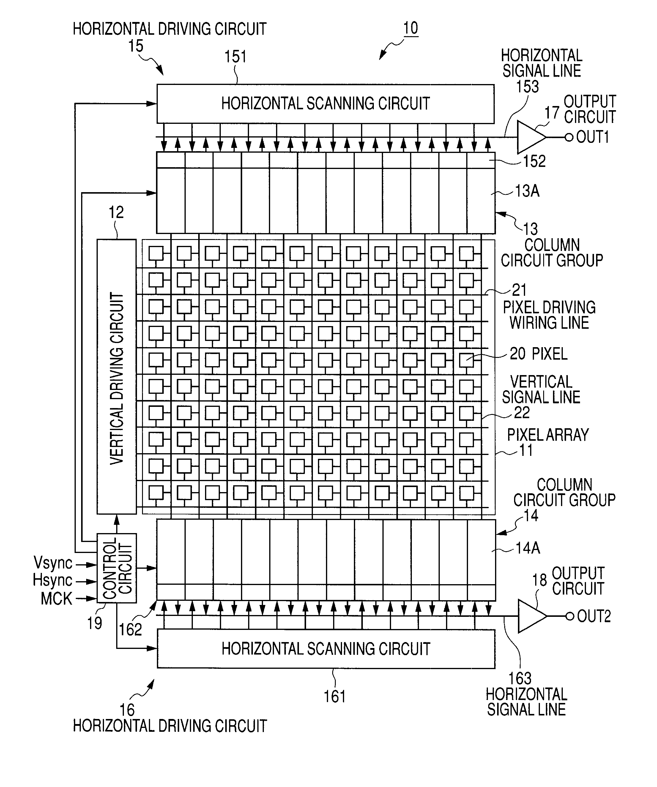
[0037]FIG. 1 is a diagram schematically illustrating the structure of a solid-state imaging device according to an embodiment of the invention. In this embodiment, a CMOS (complementary metal oxide semiconductor) image sensor is given as an example of the solid-state imaging device.

[0038] As shown in FIG. 1, a solid-state imaging device 10 according to this embodiment includes a pixel array 11, a vertical driving circuit 12, M column circuit (column parallel signal processing circuit) groups 13 and 14 (in this embodiment, M=2), horizontal driving circuits 15 and 16, output circuits 17 and 18, and a control unit 19.

[0039] In the pi...


PUM


Abstract

A physical quantity detecting device includes: a pixel array that has pixels two-dimensionally arranged in a matrix, each converting a physical quantity supplied from the outside into an electric signal; a driving circuit that scans, as read rows, N rows of pixels (N is an integer equal to or larger than 3) in the pixel array at the same time and reads out signals corresponding to the pixels in the read rows; and M signal processing circuit groups (1<M<N) each of which has M column circuits provided for each column of pixels of the pixel array, sequentially receives and processes signals output from the read rows, and when a scanning unit period is H, processes signals of the next read row within an average period of (M / N)H.

Description

CROSS REFERENCES TO RELATED APPLICATIONS [0001] The present invention contains subject matter related to Japanese Patent Application JP 2005-321753 filed in the Japanese Patent Office on Nov. 7, 2005, the entire contents of which being incorporated herein by reference. BACKGROUND OF THE INVENTION [0002] 1. Field of the Invention [0003] The invention relates to a physical quantity detecting device for detecting a physical quantity supplied from the outside, to a method of driving the physical quantity detecting device, and to an imaging apparatus using a solid-state imaging device for detecting light incident from the outside as a physical quantity. [0004] 2. Description of the Related Art [0005] A solid-state imaging device for detecting the intensity of light incident via a subject as a physical quantity or a fingerprint detecting device (capacitance detecting device) for detecting capacitance formed to correspond to a fingerprint between a detecting electrode and the surface of a ...

Claims


Application Information

Patent Timeline
Patent Type & Authority Applications(United States)
IPC IPC(8): H04N5/335H04N5/347H04N5/355H04N5/369H04N5/374H04N5/376
CPCH04N3/155H04N5/35572H04N5/374H04N25/587H04N25/589H04N25/767H04N25/745H04N25/76
Inventor MABUCHI, KEIJI
Owner SONY CORP
Why Eureka
Try Eureka