

Material for organic electroluminescence device and electroluminescence device
- Summary
- Abstract
- Description
- Claims
- Application Information
AI Technical Summary
Benefits of technology
Problems solved by technology
Method used
Image

Examples
example 1
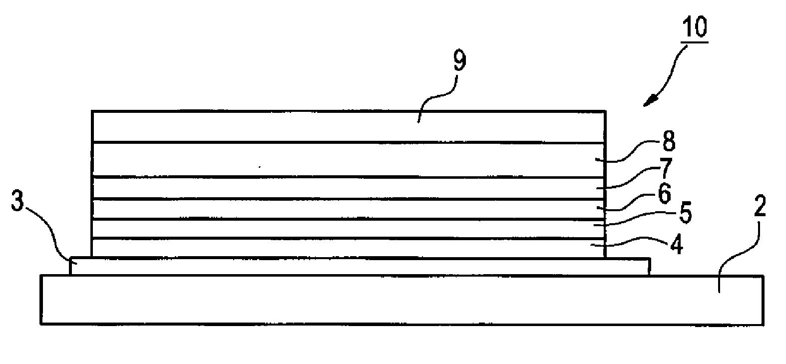
[0329]A glass substrate having an indium tin oxide (ITO) film of 100 μm thick and 2.5 cm square (manufactured by GEOMATEC, surface resistance: 10Ω / □) was placed in a washing vessel and ultrasonically washed in 2-propanol. Then, UV-ozone treatment was performed for 30 minutes. On the resulting transparent anode (ITO film), the following organic layers were successively deposited by using vacuum vapor deposition.
[0330]First layer: CuPc (copper phthalocyanine), film thickness: 120 nm
[0331]Second layer: NPD ((N,N′-di-α-naphthyl-N,N′-diphenyl)benzidine), 7 nm thick
[0332]Third layer: CBP (4,4′-di(9-carbazoyl)biphenyl)), film thickness: 3 nm
[0333]Fourth layer (light emitting layer): having Compound 1 (9 mass %) as a light emitting material (dopant) and mCBP (91 mass %) as a host material, film thickness: 30 nm
[0334]Fifth layer: first electron transport material (Balq): film thickness: 30 nm
[0335]A cathode was obtained by successively depositing, on the fifth layer, lithium fluoride and met...
example 2
[0346]Devices were prepared in a manner similar to that employed in Example 1 by using the light emitting materials shown in Table 6. Upon preparation, as soon as the materials were put in a crucible, vapor deposition was started (Vapor deposition condition 1).
[0347]Next, after the crucible containing the materials was heated for 48 hours without changing the temperature, vapor deposition was started (Vapor deposition condition 2) and a device was prepared similarly. Deposition condition 2 was performed on the assumption that a large amount of a material be vapor deposited successively upon production of devices. Brightness of the two devices thus prepared was measured by applying a voltage to give a current density of 10 mA / cm2. The brightness is expressed as a relative value supposing that the brightness of Device 2-1 is 100.
TABLE 6Brightness underBrightness underDepositionvapor depositionLight emitting materialcondition 1condition 2(content ratio)(relative value)(relative value)I...
PUM
 Abstract
Description
Claims
Application Information