Semiconductor memory device and data write method thereof

a memory device and memory technology, applied in the field of semiconductor memory devices and data write methods, can solve the problems of improving the speed of the nand-type and the difficulty of detecting data at a high ra

Active Publication Date: 2007-05-31
KIOXIA CORP
View PDF7 Cites 68 Cited by
  • Summary
  • Abstract
  • Description
  • Claims
  • Application Information

AI Technical Summary

Problems solved by technology

Recently, however, a mobile apparatus tends to deal with an image data and the like with a large quantity of data.
Even the above-described method is used, there is a limit for improving the speed of the NAND-ty

Method used


Image

  • Semiconductor memory device and data write method thereof
  • Semiconductor memory device and data write method thereof
  • Semiconductor memory device and data write method thereof

Examples


Embodiment Construction

[0071] Illustrative embodiments of this invention will be explained with reference to the accompanying drawings below.

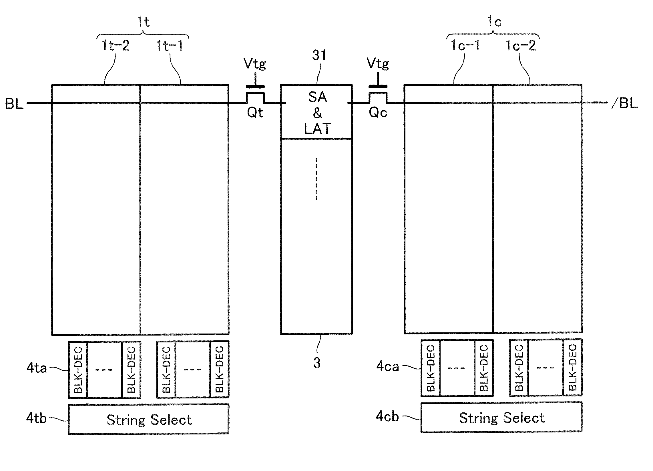
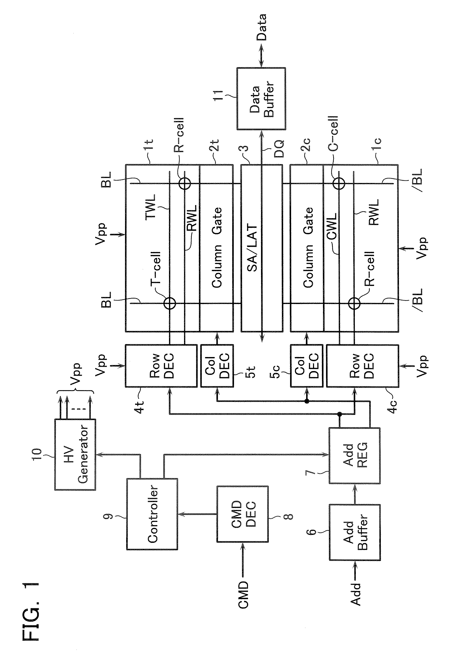
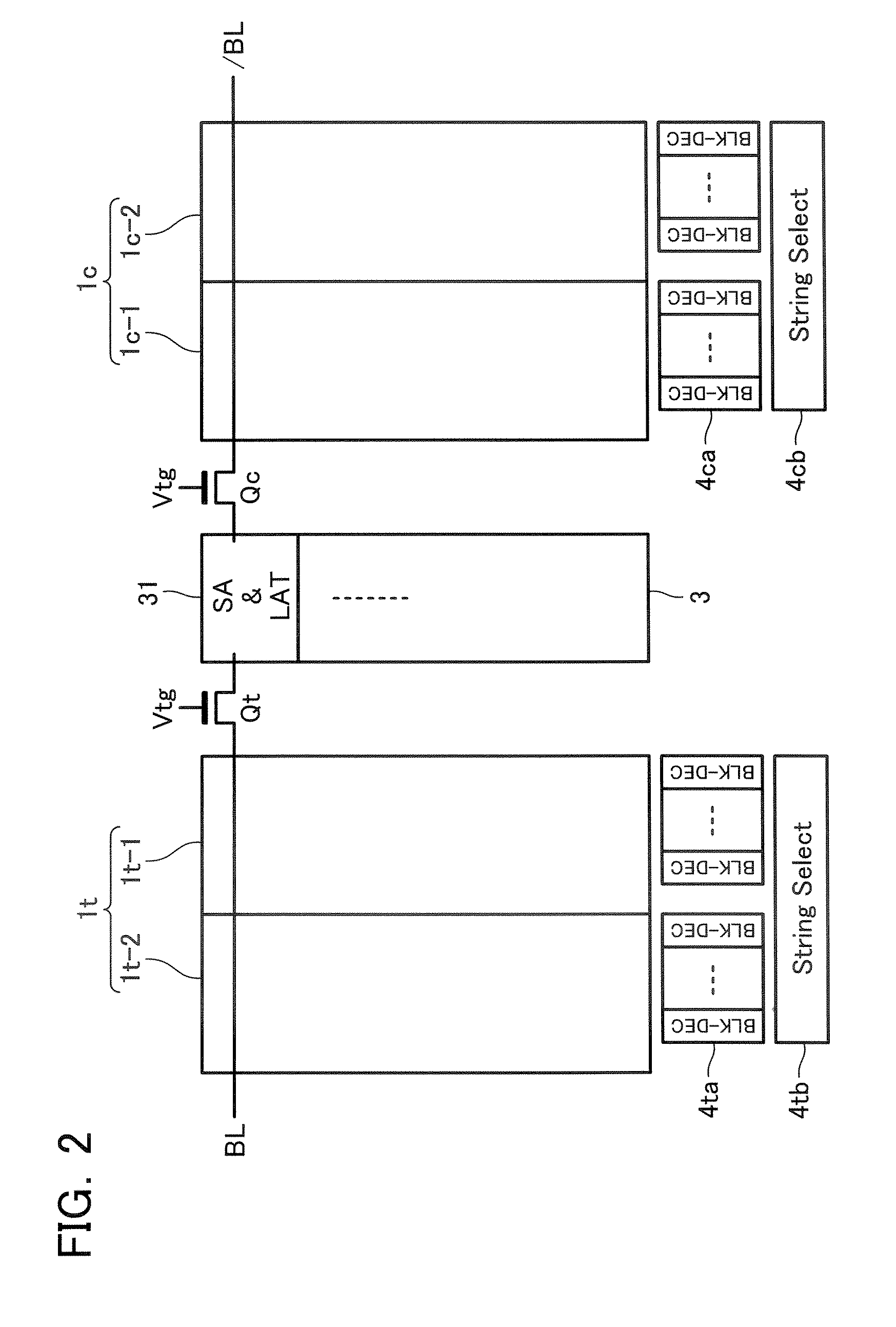
[0072] In a semiconductor memory device in accordance with this embodiment, the main portion of the memory cell array is set as an area of “information cells”, into each of which one of plural physical quantity levels (i.e., data levels) is written while the remaining portion is set as an area of “reference cell(s)”, into which a fixed physical quantity level (i.e., reference data level) is written for serving for detecting the data levels. In other words, there is prepared a common reference cell in correspondence with plural information cells, and the reference cell constitutes a pair with each of the plural information cells.

[0073] While in the embodiment described below, a four-level data storage scheme is used, the present invention is not limited to it. In case of a four-value data storage scheme, an information cell is set to have a data level selected in L0...


PUM


Abstract

A semiconductor memory device including a memory cell array and a sense amplifier, wherein the memory cell array includes: a plurality of information cells, in each of which either one of multi-level data is written; a first reference cell with the same structure and the same connection state as the information cell, in which a reference data level is written for generating a first reference current; and a second reference cell, which serves for generating a second reference current used for setting the lowest data level of the multi-level data and for setting the reference data level of the first reference cell.

Description

CROSS-REFERENCE TO RELATED APPLICATION [0001] This application is based on and claims the benefit of priority from the prior Japanese Patent Application No. 2005-335407, filed on Nov. 21, 2005, the entire contents of which are incorporated herein by reference. BACKGROUND OF THE INVENTION [0002] 1. Field of the Invention [0003] This invention relates to a semiconductor memory device (EEPROM), in which electrically rewritable and non-volatile memory cells are arranged therein, and data write method thereof. [0004] 2. Description of the Related Art [0005] EEPROM flash memories are classified in general into NAND-type and NOR-type ones. A NAND-type flash memory is formed of NAND strings (i.e., NAND cell units) each having plural memory cells connected in series in such a way that adjacent cells share source / drain diffusion layers. Therefore, the cell density is made higher than that of a NOR-type one. Besides the NAND-type flash memory has a feature with low power consumption because pl...

Claims


Application Information

Patent Timeline
IPC IPC(8): G11C16/06
CPCG11C8/04G11C11/5628G11C11/5642G11C16/0483G11C16/28G11C16/3436G11C19/00G11C2211/5621G11C2211/5634G11C16/10G11C16/26G11C16/30
Inventor TODA, HARUKI
Owner KIOXIA CORP
Why Eureka
Try Eureka