Semiconductor module and manufacturing method thereof

a technology of semiconductor modules and manufacturing methods, applied in the direction of semiconductor devices, semiconductor/solid-state device details, electrical apparatus, etc., can solve the problems of deterioration of high-frequency properties, increased materials costs, and inferior heatsinking properties of resin substrates or ceramic substrates to be used for achieving cost reduction, so as to achieve good heatsinking properties, facilitate constant setting, and suppress the effect of high-frequency properties

Inactive Publication Date: 2007-06-07
PANASONIC SEMICON SOLUTIONS CO LTD
View PDF11 Cites 7 Cited by
  • Summary
  • Abstract
  • Description
  • Claims
  • Application Information

AI Technical Summary

Benefits of technology

[0012] According to the present invention, as described above, the following effects can be achieved. That is, it is possible to suppress deterioration in high-frequency property due to a connection between a semiconductor chip and peripheral circuit components each allowing the semiconductor chip to operate, and to facilitate setting of a constant. Further, in a case that a semiconductor chip is bonded to a heatsink in a manufacturing process of a semiconductor module, it is possible to perform the bonding without outflow of a conductive material from a substrate and generation of a clearance.
[0013] Thus, according to the present invention, even in a case that a semiconductor bare chip requiring a heatsinking property must be adjoined to peripheral circuit components in view of electrical properties, a small-size semiconductor module having a good heatsinking property and a high-frequency property can be realized by a stable manufacturing method at low cost while sufficiently maintaining its reliability as a product.

Problems solved by technology

However, a semiconductor module, wherein a semiconductor chip or a semiconductor package and a surface mount component are mounted on a single substrate, has a limitation in configuration because of an increase in cost of materials for constituent elements.
A resin substrate or a ceramic substrate to be used for achieving cost reduction is inferior in heatsinking property to a metal substrate.
Otherwise, it is impossible to obtain a predetermined heatsinking property.
However, the technique in the conventional example 1 has a disadvantage that a semiconductor module to be obtained is very expensive and a method for manufacturing the semiconductor module becomes complicated.
Consequently, there arise problems that a long conductor to be used herein inhibits achievement in predetermined property (particularly, high-frequency property), and intersection of conductors leads to restraint in a manufacturing method of a semiconductor module.

Method used


Image

  • Semiconductor module and manufacturing method thereof
  • Semiconductor module and manufacturing method thereof
  • Semiconductor module and manufacturing method thereof

Examples


Embodiment Construction

[0031] Hereinafter, specific description will be given of a semiconductor module according to an embodiment of the present invention and a manufacturing method thereof with reference to the drawings.

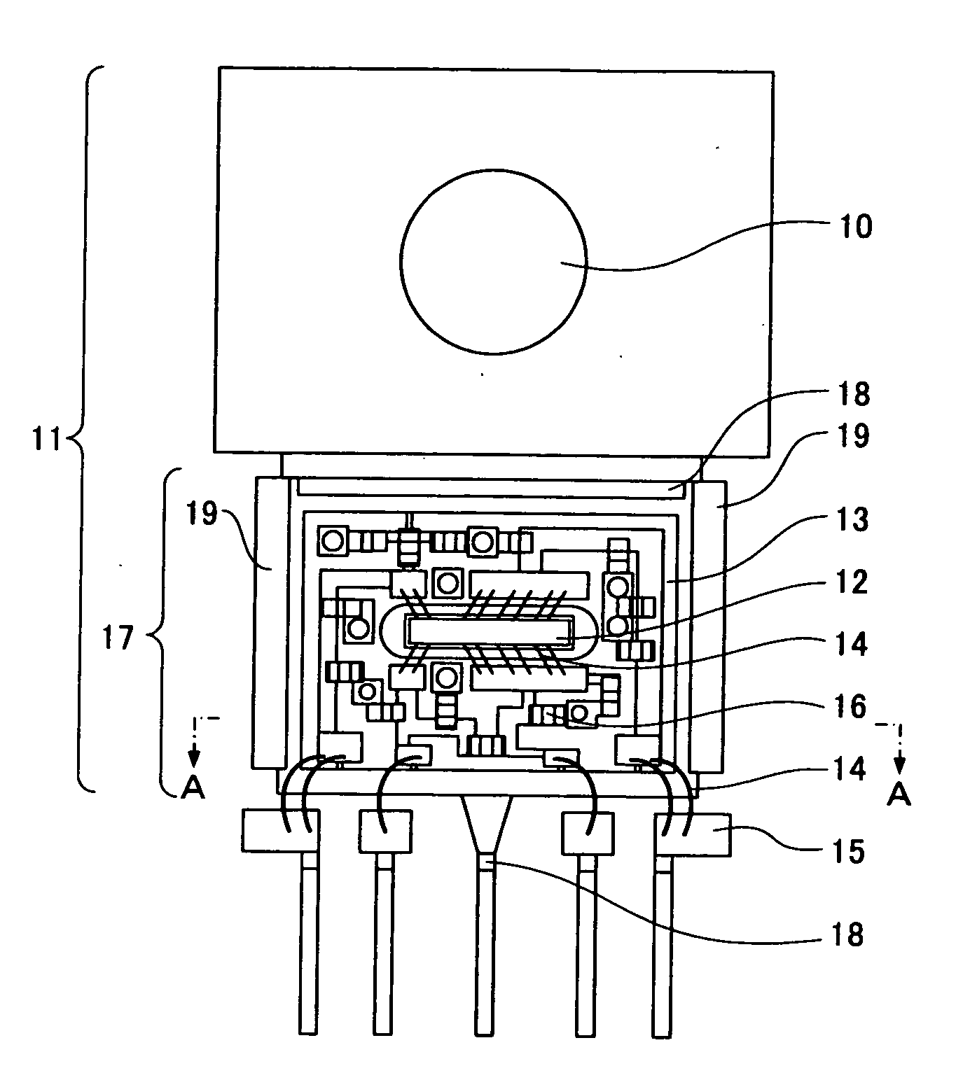
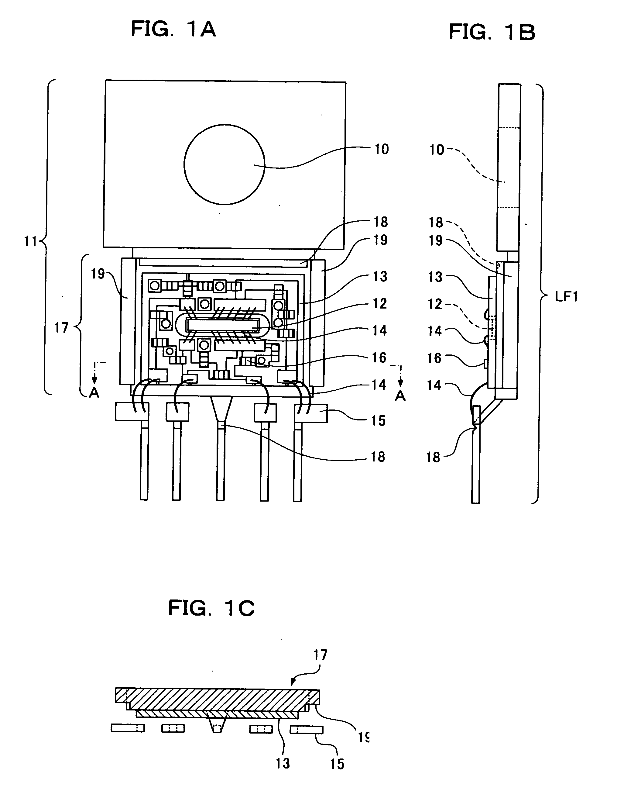
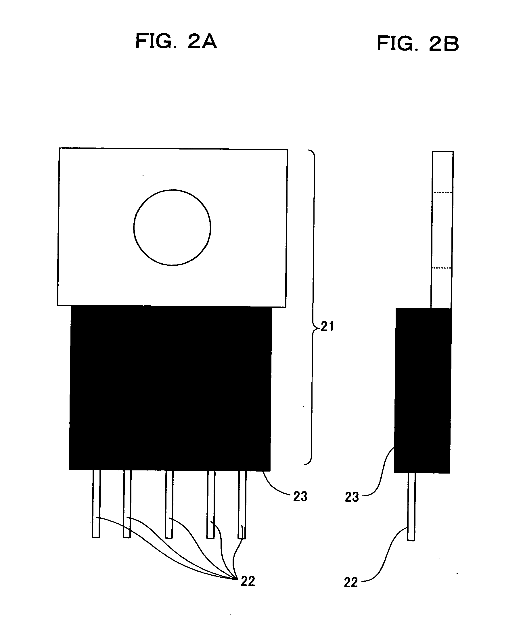
[0032]FIG. 1A is an internal front view illustrating the semiconductor module according to the embodiment. FIG. 1B is an internal side view illustrating the semiconductor module according to the embodiment. FIG. 1C is a sectional view taken along a line A-A in FIG. 1A. FIG. 2A is an external front view illustrating the semiconductor module according to the embodiment. FIG. 2B is an external side view illustrating the semiconductor module according to the embodiment. FIG. 3A is a plan view illustrating a top face of a circuit board in the semiconductor module according to the embodiment. FIG. 3B is a plan view illustrating a bottom face of the circuit board in the semiconductor module according to the embodiment. As illustrated in FIGS. 1A, 1B, 1C, 2A, 2B, 3A and 3B, the semiconductor mo...


PUM


Abstract

A center of a substrate having peripheral circuit components mounted thereon is hollowed in a size maintaining a distance for establishing a connection with a semiconductor chip through a conductor such that the semiconductor chip is bonded to a heatsink and the peripheral circuit components are arranged near the semiconductor chip so as to surround the semiconductor chip. Upon adhesion of a conductive paste material, for bonding the substrate to the heatsink having the semiconductor chip mounted thereon in a conductive manner, to a bottom face of the substrate, an adhesive tape is stuck to an edge of the substrate so as to prevent outflow of the conductive paste material, respective terminals are connected through conductors, and both the substrate and the heatsink are sealed with a resin.

Description

BACKGROUND OF THE INVENTION [0001] (1) Field of the Invention [0002] The present invention relates to a semiconductor module and a manufacturing method thereof. This semiconductor module is obtained as follows: a semiconductor chip requiring a heatsinking property and a peripheral circuit component having the heatsinking property, each mounted on a substrate, are sealed with a resin as one package. [0003] (2) Description of the Related Art [0004] Generally, it is very important to improve a heatsinking property in regard to heat generated upon operation of a semiconductor chip. In order to improve the heatsinking property, a material having good thermal conductivity is used for reducing an adverse influence of the heat generated from the semiconductor chip. A product including a substrate and a package each made of metal has a good heatsinking property. However, a semiconductor module, wherein a semiconductor chip or a semiconductor package and a surface mount component are mounted ...

Claims


Application Information

Patent Timeline
Patent Type & Authority Applications(United States)
IPC IPC(8): H01L23/34
CPCH01L23/49531H01L23/49562H01L2224/48091H01L2224/48247H01L2224/49171H01L2924/01078H01L2924/01079H01L2924/19041H01L2924/3025H01L2924/00014H01L24/48H01L24/49H01L2924/00H01L2224/45144H01L24/45H01L2224/45015H01L2924/19105H01L2924/20752H01L2224/05599
Inventor FUJIWARA, SEIJI
Owner PANASONIC SEMICON SOLUTIONS CO LTD
Why Eureka
Try Eureka