Dry etch release method for micro-electro-mechanical systems (MEMS)

Inactive Publication Date: 2007-06-07
JESSING JEFFREY R
View PDF20 Cites 10 Cited by
  • Summary
  • Abstract
  • Description
  • Claims
  • Application Information

AI Technical Summary

Benefits of technology

[0019] A major aspect of this patent is the formation of straight edges and ultra-linear sidewalls, for example, for medical devices. Medical devices, like scapels, for example, are traditionally ground using metal, alloys or diamond materials. This process often results in jagged edges, especially on a microscopic level. Also, this grinding process results in non-uniformity among different devices, and higher cost since devices must be manufactured in serial fashion. In contrast, the benefits of batch manufacturing medical devices, for example, and specifically the benefits from using the Deep Reactive Ion Etch or Bosch Process according to the method of this invention to yield the die release, include lower cost devices, ultra-linear edges, and higher degree of uniformity among devices.
[0020] The etch release method of the present invention does not generate undesirable or overly stressed die material by-products. Through novel application of Deep Reactive Ion Etching (DRIE) or Bosch etching, both being well-known dry-etch processes in the semiconductor and MEMS industries, the formation of straight edges and ultra-linear sidewalls can be achieved. These straight edges and sidewalls facilitate the clean separation of semiconductor, micromachined or MEMS die.
[0023] Another alternate aspect of the present invention is a method of creating vertical attachment tabs or webs between die by photo-resist patterning thin sections between the die prior to the dry-etch separation step. By creating these thin, vertical attachment tabs or webs between die, it allows die to remain attached to one another, but able to be broken or taken apart during a subsequent process step. This aspect also facilitates bulk micromachining or other process steps to be accomplished prior to final separation.

Problems solved by technology

To achieve release of semiconductor, micromachined or MEMS die, conventional methods such as sawing and laser scribing induce significant damage and defects that can predispose the released parts to fail both mechanically and electrically.
Dicing by-products such as silicon dust also can render parts non-functional or less functional.
These by-products are troublesome in integrated circuit manufacture, but are particularly problematic when separating MEMS structures.
This process often results in jagged edges, especially on a microscopic level.
Also, this grinding process results in non-uniformity among different devices, and higher cost since devices must be manufactured in serial fashion.

Method used


Image

  • Dry etch release method for micro-electro-mechanical systems (MEMS)
  • Dry etch release method for micro-electro-mechanical systems (MEMS)
  • Dry etch release method for micro-electro-mechanical systems (MEMS)

Examples


Embodiment Construction

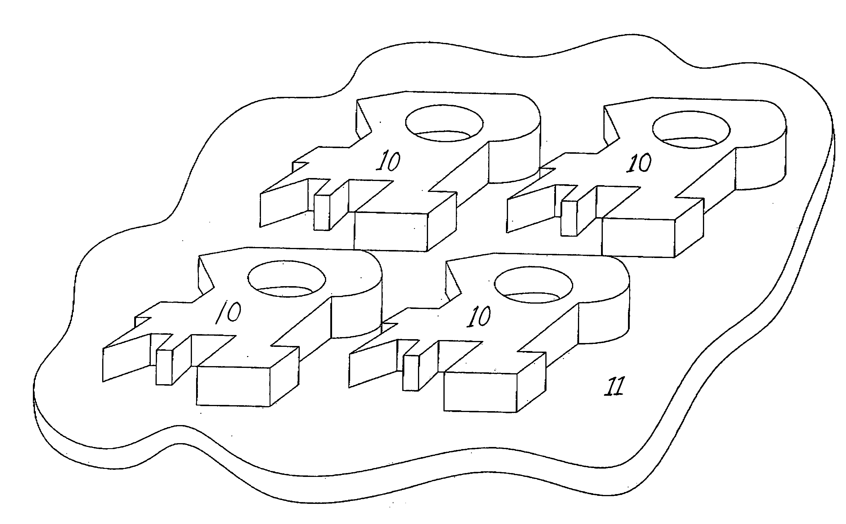
[0030] In creating semiconductor, micromachined or MEMS die, the process of dry-etching is commonly used. Several popular processes are known in the industry, such as the Bosch etching and Deep Reactive Ion Etching (DRIE) processes. In the present invention, these processes are applied in a number of novel ways, as to provide for the separation of die from one-another. It should be noted that, in the Figures, the depictions are of typical wafers, sectioned in the front along die boundaries and the sides and back as rough cutaways. In reality, entire wafers are constructed yielding a two-dimensional matrix of semiconductor, micromachined or MEMS die which can be fabricated and separated with the methods herein described.

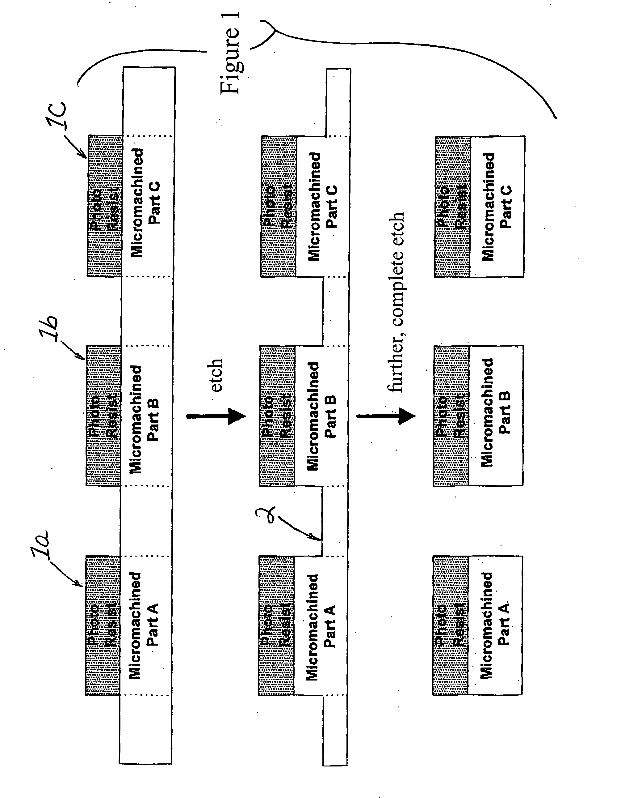
[0031] Referring to FIG. 1, there is depicted a schematic, side sectional sequence of three (3) views of the through-etch method of the present invention. In this figure, three representative micromachined die A, B, and C are shown in the top-most section view coated...


PUM


Abstract

The present invention provides a means for releasing semiconductor, micromachined and / or Micro-Electro-Mechanical Systems (MEMS) parts from a substrate. Semiconductor, micromachined or MEMS components built at the wafer level must be separated after fabrication. Through novel application of Deep Reactive Ion Etching (DRIE) or Bosch etching to etch through the substrate, full or partial separation is achieved. The formation of fine edges and ultra-linear sidewalls can be achieved, and no residues remain as a result of the process. Alternative embodiments of the present invention allow subsequent micromachining or other process steps to be accomplished, in bulk, to the bottom of the die. Other alternative embodiments involve fabrication of horizontal or vertical attachment webs or tabs between die by partial through-etching or by photo-resist patterning sections between the die prior to a dry-etch, leaving the webs or tabs.

Description

[0001] Activities related to this non-provisional patent application were conducted with funding under NSF EPSCOR #NEC6105JESS.BACKGROUND OF THE INVENTION [0002] 1. Field of the Invention [0003] This invention relates generally to fabrication of micro-electro-mechanical systems (MEMS), and more particularly to the method of dry-etched release of micromachined and / or integrated circuit parts. [0004] 2. Related Art [0005] The present invention has been shown to provide a superior method with multiple embodiments for releasing and / or separating micromachined parts and / or integrated circuits from adjacent materials that are fabricated on thin-film substrates such as silicon wafers. The inventors have found no other similar methods either in the art or commercially that offer the advantages of being a reproducible, damage-free and inexpensive way of releasing or separating of individual parts. [0006] De Juan, Jr. et al, U.S. Pat. No. 5,317,938, discloses a method of making a microsurgica...

Claims


Application Information

Patent Timeline
IPC IPC(8): H01L21/30H01L21/00H01L21/302H01L21/461
CPCB81C1/00904B81C2201/0132
Inventor JESSING, JEFFREY R.
Owner JESSING JEFFREY R
Why Eureka
Try Eureka