Liquid crystal display device and method for driving the same

a display device and liquid crystal technology, applied in the direction of instruments, static indicating devices, etc., can solve the problems of low response speed, low image quality, and display panels that show unwanted trails

Inactive Publication Date: 2007-06-14
TOSHIBA MATSUSHITA DISPLAY TECH
View PDF12 Cites 50 Cited by
  • Summary
  • Abstract
  • Description
  • Claims
  • Application Information

AI Technical Summary

Benefits of technology

[0132] said backlight control unit controls a current of said backlight to increase so that the backlight lights brighter when said timing to start lighting of a backlight delays.
[0145] According to the 11th to 20th present invention, transferring from the bend alignment to the spray alignment is prevented from occurring in a method for causing the backlight to illuminate only during a period in which a liquid crystal display panel responds to display data even at a high temperature.

Problems solved by technology

However, currently popular TN (Twisted Nematic) oriented liquid crystal display panels offer small view angles and low response speeds and may show unwanted trails during motion picture display.
These liquid crystal display panels thus offer lower image quality than cathode-ray tubes.
There is a problem, however, in that insufficient writing to the liquid crystal display element is apt to occur when a voltage corresponding to black data to be inserted for preventing transferring from the bend alignment to the spray alignment is supplied with a method for causing a backlight to light only while the liquid crystal display element responds to the display data as described in FIG. 29 and FIG. 30.
If the panel has a low temperature, there is another problem in that the contrast lowers due to insufficient writing of black data for preventing transferring from the bend alignment to the spray alignment to the liquid crystal display element.
If the panel has a high temperature, there is a problem in transferring from the bend alignment to the spray alignment of the liquid crystal display element occurs.
The conventional method for causing the backlight to illuminate only while the liquid crystal display element responds to the display data has a problem that occurs when the temperature of the liquid crystal display element lowers below a certain temperature and a problem that occurs when the temperature of the liquid crystal display element rises above another certain temperature.
That may cause insufficient writing to the liquid crystal display element when the black data is written.
Thus, the problem occurs when the temperature is below a certain temperature.
Thus, if the liquid crystal display element is not charged to a required voltage value while the gate pulse is occurring, insufficient writing occurs.
When white display that is difficult to be written in the liquid crystal display element is provided, the liquid crystal display element is not charged to the predetermined voltage value while a gate pulse for a black writing period occurs, resulting in transferring from the bend alignment to the spray alignment due to insufficient writing as shown in “when white display is provided” of FIG. 31.

Method used


Image

  • Liquid crystal display device and method for driving the same
  • Liquid crystal display device and method for driving the same
  • Liquid crystal display device and method for driving the same

Examples


embodiment 1

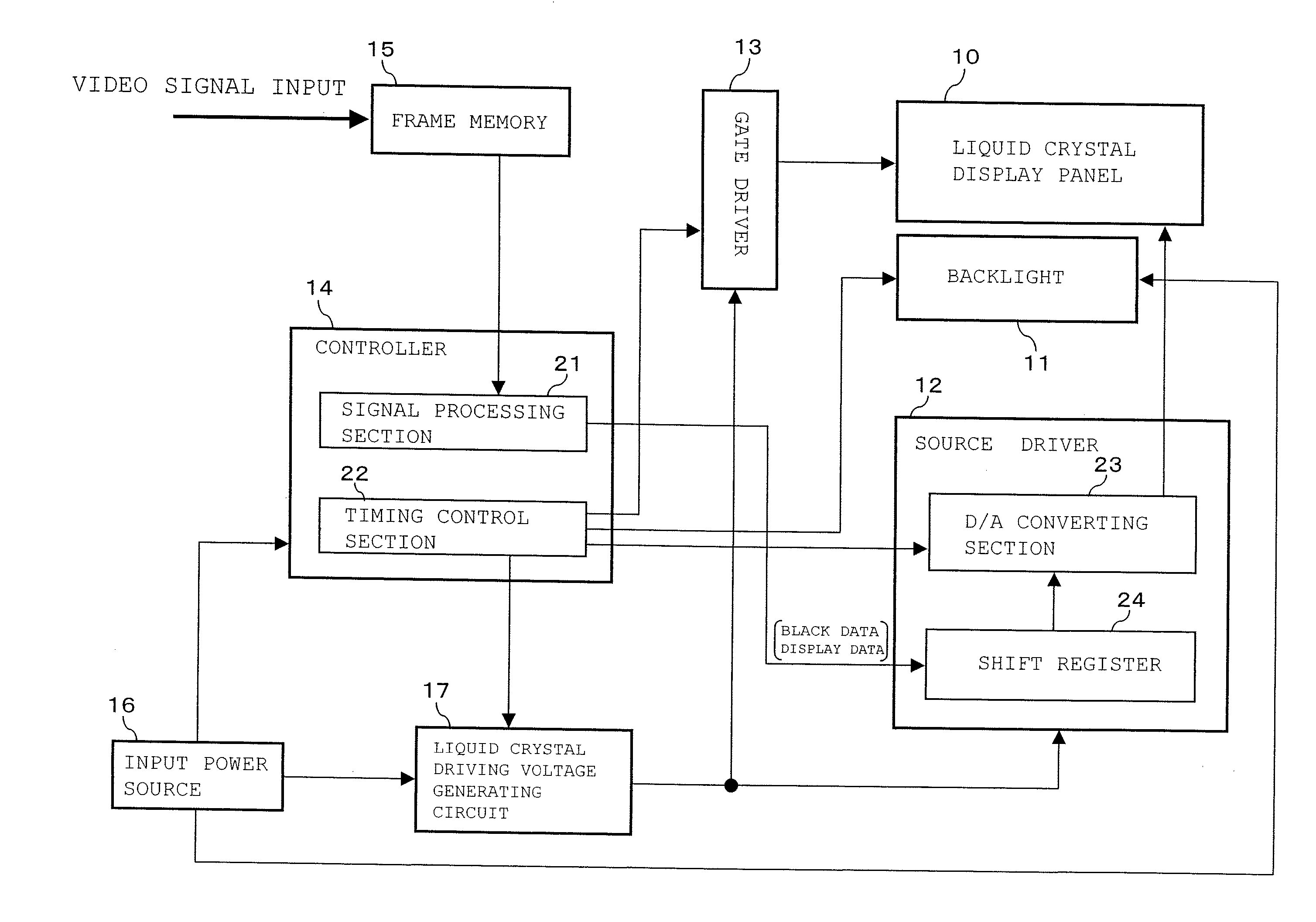
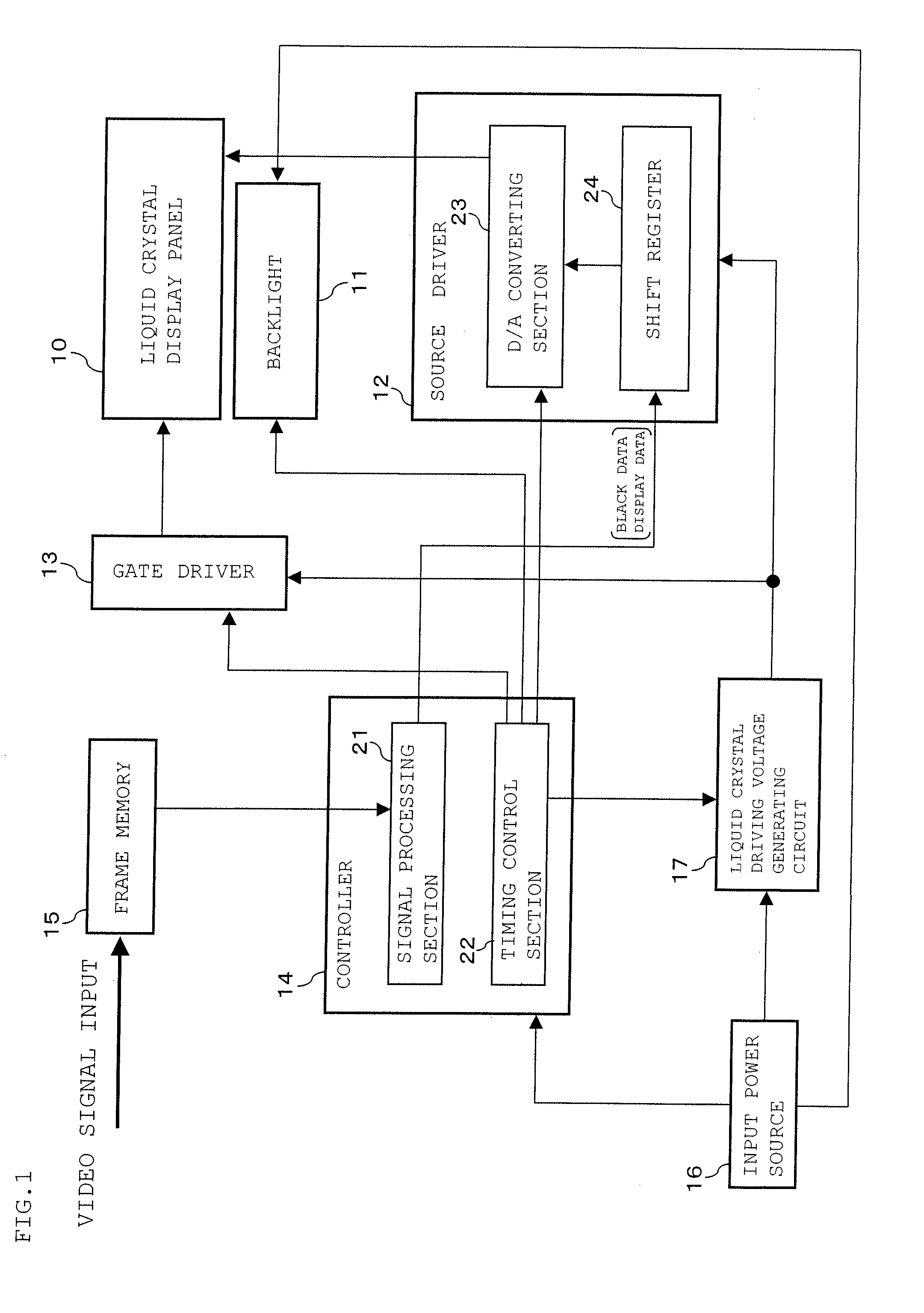
[0215]FIG. 1 is a block diagram showing a configuration of a liquid crystal display device according to Embodiment 1 of the present invention.

[0216] The liquid crystal display device according to Embodiment 1 includes a liquid crystal display panel 10, a backlight 11, a source driver 12, a gate driver 13, a controller 14, a frame memory 15, an input power source 16, and a liquid crystal driving voltage generating circuit 17.

[0217] The liquid crystal display panel 10 comprises signal lines and scan lines arranged in a matrix and an OCB mode liquid crystal display element provided on an intersection point between them.

[0218] The backlight 11 is arranged at the backside of the liquid crystal display panel 10 for illuminating the liquid crystal display panel 10 with a plurality of short afterglow type cold cathode tubes.

[0219] The frame memory 15 is a storage section, which temporally stores data of an immediately previous field of inputted video signal data.

[0220] The input power ...

embodiment 2

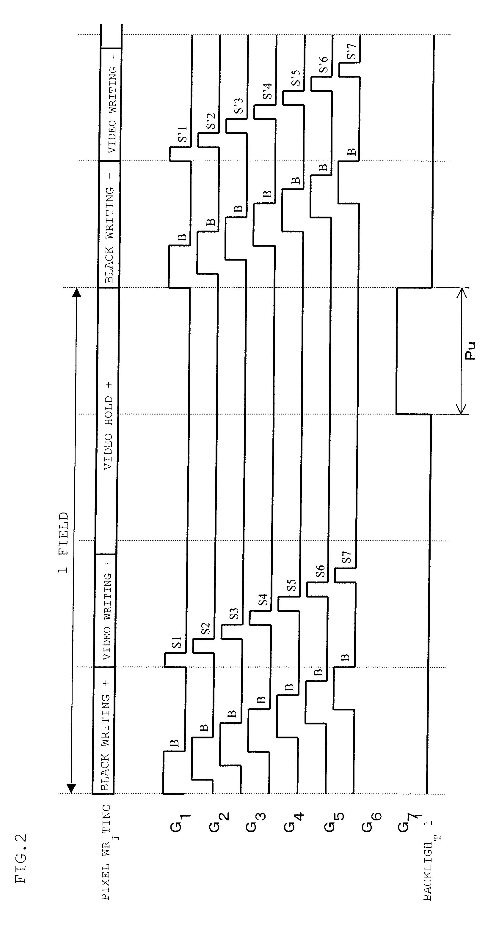
[0254] Description will be given below of a display operation of the liquid crystal display device according to Embodiment 2 of the present invention.

[0255] The liquid crystal display device according to Embodiment 2 has the same configuration as that of the liquid crystal display device according to Embodiment 1 and as shown in FIG. 1. The controlling on the gate driver 13 of the timing control section 22 is different from that of the liquid crystal display device according to Embodiment 1.

[0256] In FIG. 2, the timing when a gate pulse is generated during the black writing period only needs to be a timing when a period for keeping a voltage for black data for preventing transferring from the bend alignment to the spray alignment to be charged is the minimum for preventing transferring from the bend alignment to the spray alignment or more for each liquid crystal display element (a period during which transferring from the bend alignment to the spray alignment does not occur if on...

embodiment 3

[0270] Description will be given below of a display operation of the liquid crystal display device according of Embodiment 3 of the present invention.

[0271] The liquid crystal display device according to Embodiment 3 has the same configuration as that of the liquid crystal display device according to Embodiment 1 as shown in FIG. 1. The controlling on the gate driver 13 of the timing control section 22 is different from that of the liquid crystal display device according to Embodiment 1.

[0272] In the embodiments 1 and 2, a voltage to be supplied to the liquid crystal display element is reversed for each field, and thus, the gate pulse width when black data for preventing transferring from the bend alignment to the spray alignment is written is increased for all the fields. If data is continuously written at a voltage with the same polarity, less insufficient writing occurs than in the case where the data is written with the polarity reversed. For the liquid crystal display device ...


PUM


Abstract

Occurrence of insufficient writing to a liquid crystal display element is prevented in the liquid crystal display device which causes a backlight to illuminate only while the liquid crystal display element responds to the display data. A liquid crystal display device has a liquid crystal display panel using an OCB mode liquid crystal, divides a field period into a black writing period, a display data writing period, and a display data hold period, writes black data for preventing transferring from the bend alignment to the spray alignment in the black writing period, writes display data in the display data writing period, and lights a backlight during a part of the display data hold period, wherein a gate driver makes periods during each of which each of gate signals corresponding to each of the scan lines are turned on are same to each other when a source driver writes the display data in the liquid crystal display element, and makes periods during each of which each of gate signals corresponding to each of the scan lines are turned on longer than a period during which display data is written for a line when the source driver writes black data for preventing transferring from the bend alignment to the spray alignment.

Description

CROSS-REFERENCE TO RELATED APPLICATIONS [0001] This application claims priority to Japanese Patent Application Nos. 2005-358175, filed in the Japanese Patent Office on Dec. 12, 2005, 2005-358186, filed in the Japanese Patent Office on Dec. 12, 2005, and 2006-190697, filed in the Japanese Patent Office on Jul. 11, 2006, the entire contents of each are hereby incorporated herein by reference. BACKGROUND OF THE INVENTION [0002] 1. Field of the Invention [0003] The present invention relates to a liquid crystal display device using an OCB mode liquid crystal and a method for driving the liquid crystal display device. [0004] 2. Description of the Related Art [0005] Liquid crystal display devices are thin and light and are expected to replace conventional cathode-ray tubes. Thus, the applications of liquid crystal display devices have been increasingly expanded. However, currently popular TN (Twisted Nematic) oriented liquid crystal display panels offer small view angles and low response s...

Claims


Application Information

Patent Timeline
Patent Type & Authority Applications(United States)
IPC IPC(8): G09G3/36
CPCG09G3/3406G09G2310/06G09G2310/062G09G2310/063G09G2320/0238G09G2320/041G09G2330/045G09G2360/18
Inventor KAWAGUCHI, SEIJI
Owner TOSHIBA MATSUSHITA DISPLAY TECH
Why Eureka
Try Eureka