
Method of manufacturing liquid crystal display panel and apparatus for cutting liquid crystal display panel

a technology of liquid crystal display panel and manufacturing method, which is applied in the direction of manufacturing tools, non-linear optics, instruments, etc., can solve the problems of degrading the display quality grinding of the cut portions of the substrate of the lcd panel, and affecting so as to achieve the effect of reducing the load applied to the lcd panel, and increasing the yield of the liquid crystal display panel

Inactive Publication Date: 2007-06-14
NEC LCD TECH CORP
View PDF10 Cites 7 Cited by
  • Summary
  • Abstract
  • Description
  • Claims
  • Application Information

AI Technical Summary

Benefits of technology

[0008] Consequently, an exemplary feature of the invention is to provide a method of cutting a pair of substrates and an apparatus for cutting a pair of substrates. The method and the apparatus make it possible to suppress incidence of chipping on the substrate, and to increase a yield of a panel.
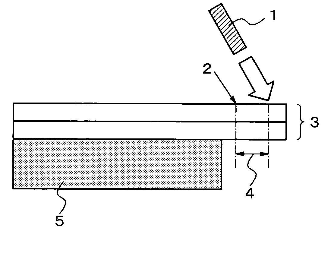
[0025] In the present invention, a liquid crystal display panel is cut in the following manner. Scribe lines are formed respectively in positions on upper and lower surfaces of the end portion of the pair of substrates. The positions correspond to each other, and the end portion protruding from the supporting stage. The liquid crystal display panel is cut by use of the principle of “leverage” and a self weight of the liquid crystal display panel. Specifically, a load is applied from a vertical or oblique direction to a predetermined position. The predetermined position is at the side of the scribe lines, and is closer to starting points of the respective scribe lines, the side being closer to the predetermined edge of the pair of substrates. Because the load applied to the liquid crystal display panel can be thereby made small, chipping due to mutual grinding of cut portions of one of glass substrates of the liquid crystal display panel can be suppressed. Thereby, a yield of the liquid crystal display panel can be increased.
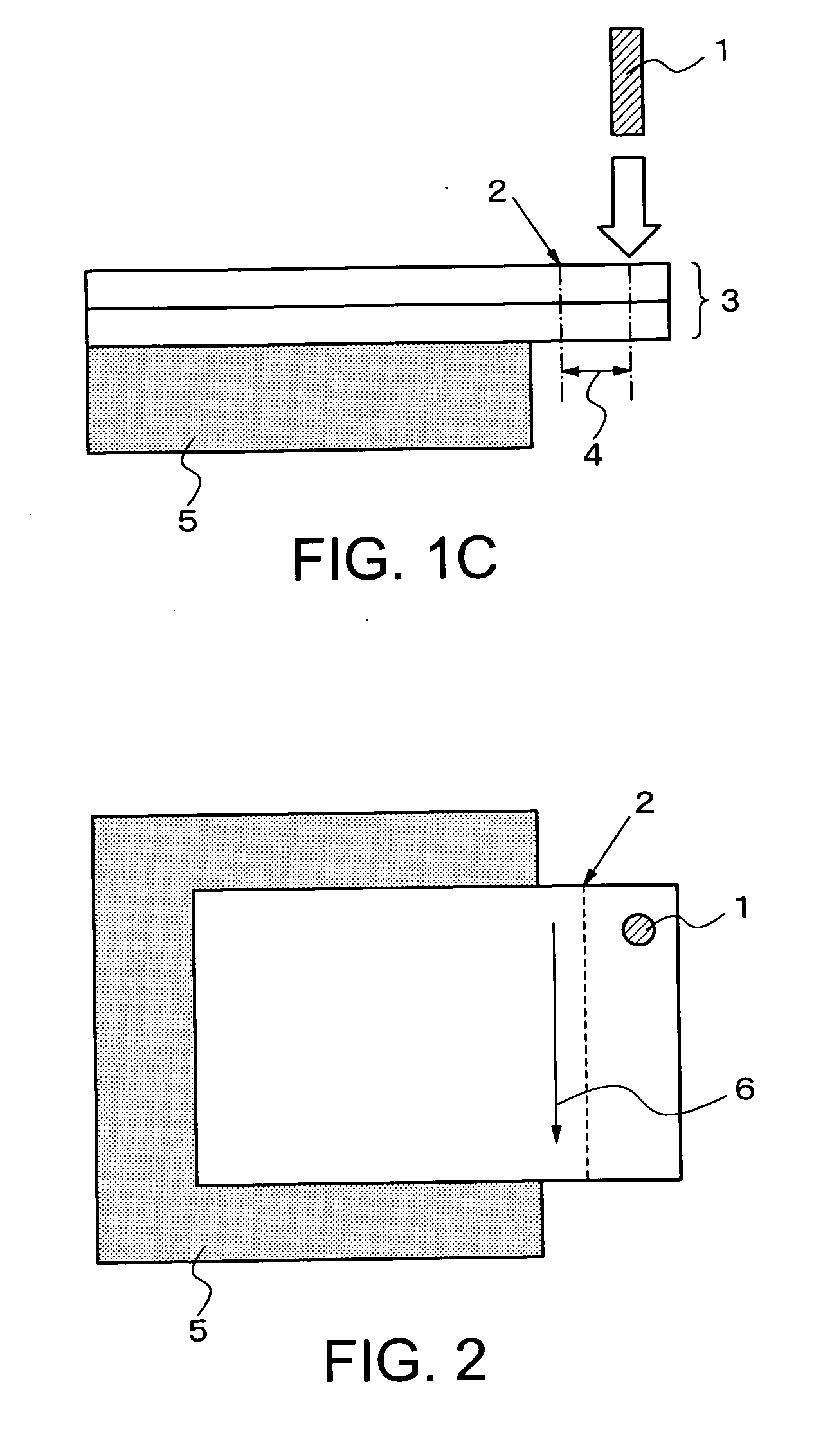
[0026] According to the method of manufacturing a liquid crystal display panel of the present invention, chipping due to mutual grinding of cut portions of the substrate of the liquid crystal display panel can be suppressed. Thereby, a yield of the liquid crystal display panel can be increased. A reason for this is as follows. When the pair of substrates of the liquid crystal display panel is cut, the pair of substrates is fixed to the supporting stage by vacuum holding in a state of overhanging the supporting stage (a state where one of end portions of the pair of substrates protruding from the supporting stage). Then, scribe lines are formed respectively on both of upper and lower substrates of the liquid crystal display panel by scribing, from upper and lower directions, positions where the pair of substrates overhangs. Thereafter, a load is applied to a predetermined position from a vertical or an oblique direction. The predetermined position is at a side of the scribed lines, and is closer to starting points of the respective scribe lines, the side being closer to the predetermined edge of the pair of substrates. Accordingly, the load applied to the liquid crystal display panel can be made small.
[0027] According to the apparatus for cutting a liquid crystal display panel of the present invention, chipping due to mutual grinding of cut portions of one of glass substrates of the liquid crystal display panel can be suppressed. Thereby, a yield of the liquid crystal display panels can be increased. A reason for this is as follows. When a pair of substrates of the liquid crystal display panel is cut, the pair of substrates is fixed to a supporting stage in vacuum holding in a state of overhanging the supporting stage (a state where one of end portions of the pair of substrates protruding from the supporting stage). Then, scribe lines are formed respectively on both of upper and lower substrates of the liquid crystal display panel by scribing, from upper and lower directions, positions where the pair of substrates overhangs. Thereafter, with a break pin, a load is applied to a predetermined position from a vertical or an oblique direction. The predetermined position is at a side of the scribe lines, and is closer to starting points of the respective scribe lines, the side being closer to the predetermined edge of the pair of substrates. Accordingly, the load applied to the liquid crystal display panel can be made small.

Problems solved by technology

However, when the cutting is performed with the above-described method of the related art, there arises a problem that, at the time of the second cutting, cut portions of the initially-cut substrate of the LCD panel grind against each other, and thereby chipping occurs thereon.
As a result, the movements of contraction and release lead to the grinding of the cut portions of the substrate of the LCD panel.
As a result, display quality of the LCD panel is degraded, and it results in a decreased yield of the LCD panels.

Method used


Image

  • Method of manufacturing liquid crystal display panel and apparatus for cutting liquid crystal display panel
  • Method of manufacturing liquid crystal display panel and apparatus for cutting liquid crystal display panel
  • Method of manufacturing liquid crystal display panel and apparatus for cutting liquid crystal display panel

Examples


first embodiment

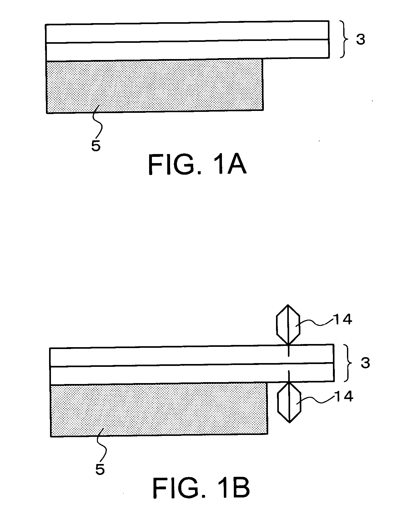
[0050] With reference to FIGS. 1A to 4, descriptions will be provided for a method of manufacturing an LCD panel and an apparatus for cutting an LCD panel according to a first exemplary embodiment of the present invention.

[0051] An LCD panel to be cut with the method of the present invention is composed of an active-matrix substrate on which switching elements, such as thin-film transistors (TFTs), are formed; a counter substrate facing the active-matrix substrate; and a liquid crystal layer interposed and held between the two substrates. In order to reduce manufacturing costs of the LCD panels, a commonly-used method is that, after each of the active-matrix and counter substrates has been prepared by using a glass substrate of a large size, the two substrates are bonded to each other by using a sealing material and the like. Then, the pair of substrates bonded to each other is cut into predetermined dimensions in accordance with a size of a product to be manufactured. Then, an LCD...

second embodiment

[0069] Next, a method of cutting an LCD panel and an apparatus for cutting an LCD panel according to a second exemplary embodiment of the present invention will be described with reference to FIGS. 5A to 5C and FIG. 6. Although a load is applied from a vertical direction by using the break pin 1 in the first embodiment, the second embodiment is characterized by applying a load from an oblique direction.

[0070] The apparatus for cutting the LCD panel in the second embodiment includes a supporting stage 5, a pair of scribe cutters 14 and a break pin 1. The LCD panel is fixed to the supporting stage 5 by vacuum holding. The scribe cutters 14, as a pair, are respectively arranged in predetermined positions outside a plane of the supporting stage 5. The break pin 1 is arranged in a predetermined position outside the plane of the supporting stage 5. The supporting stage 5 and the pair of scribe cutters 14 are identical to those of the first embodiment.

[0071] In the second embodiment, wit...


PUM

PropertyMeasurementUnit
distanceaaaaaaaaaa
distanceaaaaaaaaaa
thicknessaaaaaaaaaa

Abstract

A liquid crystal display (LCD) panel is fixed to a supporting stage by vacuum holding in a way that an end portion of a predetermined one of edges of the pair of substrates protrudes from the supporting stage. Next, scribe lines are formed respectively in positions on upper and lower surfaces of the end portion of the pair of substrates, and the end portion protruding from the supporting stage. Thereafter, a load is applied to a predetermined position by using a break pin. The load is applied to the predetermined position at a side of the scribe lines toward the outside closer to starting points of the respective scribe lines. Accordingly, the LCD panel is cut.

Description

BACKGROUND OF THE INVENTION [0001] 1. Field of the Invention [0002] The present invention relates to a method of manufacturing a liquid crystal display (LCD) panel, and an apparatus for cutting the LCD panel. Particularly, the present invention relates to a method of cutting a pair of substrates bonded to each other, and to an apparatus for cutting the pair of substrates. [0003] 2. Description of the Related Art [0004] LCD devices are utilized in a wide range of fields, including Office Automation (OA) equipment, Audio and Visual (AV) equipment and portable terminal equipment, owing to characteristics thereof of thin profile, light weight, and low power consumption. These LCD devices are each composed of an LCD panel including a pair of glass substrates holding liquid crystal material interposed therebetween; a backlight for lighting the LCD panel; and the like. In order to reduce manufacturing cost of the LCD panel, the LCD panel is manufactured in the following manner. Each of the...

Claims


Application Information

Patent Timeline
Patent Type & Authority Applications(United States)
IPC IPC(8): G02F1/1339
CPCB65G2249/04C03B33/033C03B33/07G02F1/133351Y02P40/57Y10T225/12
Inventor MORI, MAKOTO
Owner NEC LCD TECH CORP
Learn More